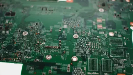

Recent advancements in the manufacturing of printed circuit boards (PCBs) have turned towards adopting sustainable and recyclable materials, aiming to mitigate the environmental impact and high energy consumption traditionally associated with PCB production. These innovations are driven not only by regulatory frameworks but also by corporate commitments to sustainability. The momentum towards greener practices is becoming increasingly important as environmental concerns continue to rise within the electronics industry.
Current Challenges and Traditional Methods
The Status Quo of PCB Manufacturing
PCBs are typically produced using FR4, a glass-reinforced epoxy resin laminate favored for being lightweight, strong, and cost-effective. However, FR4 presents a significant environmental challenge. Despite its positive properties, FR4 is non-recyclable, which contributes considerably to environmental waste. Manufacturers extensively use it due to its viability, but neglect the long-term ramifications and ecological footprint. The traditional methods of PCB manufacturing further exacerbate environmental pollution, largely because they do not adequately address the disposal issues surrounding non-recyclable materials.
The environmental burden of FR4 does not stem solely from its non-recyclable nature. The production process itself often involves significant energy consumption and emissions that contribute to greenhouse gases. The cost-effectiveness of FR4 has historically overshadowed these environmental costs, but as the push for sustainability gains traction, the focus is shifting towards more holistic methods that encompass both economic and ecological aspects. Transitioning from FR4 to more sustainable alternatives requires substantial changes in industry practices, but it is a necessary step to reduce the sector’s overall footprint.
Environmental Hazards of FR4
One of the primary environmental concerns regarding FR4 is the presence of toxic halogenated flame retardants within its composition, which become particularly hazardous when the material is incinerated. The decomposition of these chemicals releases harmful substances into the environment, contributing significantly to air and soil pollution. Burning FR4 at the end of its life cycle exacerbates these hazards, posing risks to both human health and ecosystems. The mounting issue of electronic waste (e-waste) has highlighted the urgent need for alternative materials that minimize such risks.
The urgency for more environmentally friendly alternatives in PCB construction cannot be overstated. As the volume of e-waste continues to grow globally, finding sustainable solutions to replace FR4 has become critical. Various stakeholders, including manufacturers, policymakers, and environmental organizations, are increasingly advocating for materials that reduce toxic emissions and are not purely driven by short-term financial gains. The transition involves both technological innovation and a shift in regulatory frameworks to promote the adoption of safer, greener materials in electronics manufacturing.
Innovations in Substrates
Introduction of Biodegradable Substrates
In response to the environmental hazards posed by traditional PCB materials, new biodegradable substrates like JIVA’s Soluboard® have emerged as promising alternatives. Made from flax and jute fibers, Soluboard® is designed to dissolve in hot water, which facilitates efficient recycling of components and recovery of precious metals. This innovative approach is gaining traction and is being tested by leading companies such as Microsoft, Infineon, and Jaguar. These trials are part of a broader industry effort to address the rising levels of global e-waste and reduce reliance on non-recyclable materials.
Soluboard®’s entire lifecycle is indicative of a sustainable approach to PCB manufacturing. From its production from renewable resources to its ultimate dissolution and component reclamation, Soluboard® offers a comprehensive solution to the environmental challenges associated with traditional substrates. This biodegradability reduces the impact on landfills and the associated toxins released into the soil and air. As more companies recognize the importance of minimizing their ecological footprints, the adoption of such advanced materials is likely to increase, setting new standards for the industry.
Flexible and Biodegradable Alternatives
Polylactic acid is another innovative substrate gaining attention for flexible PCBs. Derived from organic industrial waste, polylactic acid is biodegradable and presents a sustainable alternative to conventional materials like plastic polyimide. Although it endures lower maximum temperatures (up to 140°C) compared to polyimide and FR4, polylactic acid remains compatible with existing manufacturing processes, including silver ink sintering. This material is currently undergoing prototype validation by various companies and research institutions, indicating its potential for broader application in the industry.
The development of polylactic acid for PCBs underscores the broader trend towards sustainable manufacturing practices in the electronics sector. Biodegradable alternatives like polylactic acid not only reduce dependence on fossil fuels but also lessen the environmental impact during disposal. The ongoing research and validation processes suggest that these sustainable substrates could soon become viable options for mainstream PCB manufacturing. As their commercial readiness approaches, these materials are set to play a critical role in transforming the way electronics are produced and disposed of, ultimately contributing to a reduction in the industry’s carbon footprint.
Sustainable Soldering Practices
Utilizing Recycled Tin
Soldering is a crucial process in PCB manufacturing that has significant environmental implications, particularly due to the reliance on primary tin sourced from ecologically damaging mines in locations like China, Indonesia, and Myanmar. Mayerhofer Elektronik has demonstrated the viability of using second-life tin, which offers a sustainable solution to this issue. Recycled tin is produced by smelting waste metal and metal oxide, and it maintains the same quality as primary tin, as confirmed by X-ray diffraction methods. With the electronics industry consuming about 180,000 tonnes of primary tin annually, transitioning to recycled tin could substantially reduce the environmental burden associated with tin mining.
The use of recycled tin in soldering also aligns closely with the principles of a circular economy, where materials are reused and recycled rather than disposed of. Despite the current recycling rate of tin being only around 30%, there is considerable potential for improvement. Encouraging the use of recycled tin not only helps to reduce the environmental footprint of the electronics industry but also supports the development of more sustainable supply chains. As more companies adopt this practice, the demand for new tin mining could decrease, leading to less environmental degradation and promoting more responsible resource management.
Regulatory Encouragement for Metal Recycling
Regulatory frameworks are playing a crucial role in promoting sustainable soldering practices and increasing the recycling rate of metals like tin. Germany’s National Circular Economy Strategy, introduced in the current year, aims to halve per capita raw material consumption by 2045. This strategy provides incentives for companies to incorporate secondary materials into their products. Apple has set a precedent by committing to using secondary tin in all its products by 2035, demonstrating that large-scale adoption of recycled metals is feasible and can be accelerated.
Such regulatory initiatives underscore the importance of government intervention in driving industry-wide change. By setting ambitious goals and providing the necessary support for companies to meet these targets, policymakers can facilitate a smoother transition towards sustainable practices. Encouragement for recycling and secondary metal usage can help overcome initial cost barriers and promote widespread adoption. As more companies commit to these practices, the electronics industry can move towards a more sustainable and environmentally responsible future, reducing its reliance on primary, non-renewable resources.
Addressing Copper Waste
Traditional Copper Etching Practices
The traditional processes involved in PCB manufacturing, particularly copper etching, contribute to significant material wastage and environmental harm. The method entails applying a flat sheet of copper to the substrate, followed by drilling holes and etching away excess copper. This process typically results in the wastage of up to 70% of the initial copper due to the large volumes of chemical etchants like ferric (III) chloride and cupric (II) chloride required. This not only results in the loss of valuable resources but also leads to the disposal of hazardous chemicals, adding to environmental pollution.
The copper waste issue highlights the need for more sustainable etching practices. The chemicals used in the etching process pose a risk to both human health and the environment, given their potential to contaminate water and soil. Additionally, the inefficiency of the current method results in substantial economic losses due to wasted materials. Addressing these challenges is vital for creating more sustainable and cost-effective manufacturing processes. The industry’s shift towards more efficient and eco-friendly techniques can significantly reduce its overall environmental impact, aligning with broader goals of sustainability and resource conservation.
Potential Solutions for Copper Waste Reduction
Additive manufacturing is emerging as an effective solution for minimizing copper waste in PCB production. This method involves applying copper only where it is needed, substantially reducing the volume of material used. Additionally, etchant regeneration systems have been developed to recover both the etched copper and the etchant chemicals, creating a closed-loop system. These systems, which have been available for over a decade, offer significant advantages, including a payback period ranging from 6 to 18 months and the ability to considerably extend the lifespan of etchants. For example, the lifetime of ferric (III) chloride can be tripled, and hydrochloric acid consumption can be reduced by about 95%.
Implementing these advanced techniques can transform the way PCBs are manufactured, making the process less wasteful and more environmentally friendly. By recovering and recycling both the copper and the chemicals used in etching, manufacturers can reduce their reliance on new materials and minimize their environmental footprint. These improvements are not only environmentally beneficial but also economically advantageous, providing cost savings and promoting a more sustainable production model. The adoption of such technologies represents a significant step forward in the industry’s efforts to develop greener and more efficient manufacturing practices.
A Holistic View of Sustainable PCBs
Environmental Benefits of New Materials
The shift to biodegradable and recyclable materials in PCB manufacturing offers considerable environmental advantages. These new materials are generally less harmful than their traditional counterparts and contribute significantly to reducing the mounting issue of e-waste. By incorporating renewable resources and focusing on the end-of-life process, these innovations address multiple stages of the product lifecycle. Reducing the toxicity and increasing the recyclability of PCBs help in mitigating the harmful impacts on both human health and the environment, paving the way for a more sustainable electronics industry.
Adopting these advanced materials supports a circular economy model where resources are reused rather than discarded. This approach helps to conserve natural resources, reduce landfill usage, and decrease the pollution associated with the extraction and processing of raw materials. As more manufacturers recognize the benefits of sustainable materials, the industry can expect to see a shift towards practices that not only balance economic and environmental concerns but also promote long-term ecological health. This holistic view emphasizes the importance of integrating sustainability into every aspect of electronics manufacturing.
Transition Challenges and Future Prospects
Recent progress in the manufacturing of printed circuit boards (PCBs) has significantly focused on embracing sustainable and recyclable materials to reduce environmental impact and the traditionally high energy consumption tied to PCB production. This shift is propelled by not only regulatory guidelines but also strong corporate commitments to sustainability. Industry leaders are becoming increasingly aware of the importance of reducing their carbon footprints and investing in eco-friendly practices. The drive towards greener methods isn’t just a trend, but a necessary evolution as environmental concerns gain prominence within the electronics sector. Many companies are adopting innovative technologies and materials that offer lower environmental costs without compromising performance. These efforts reflect a growing acknowledgment of the role corporate responsibility plays in global environmental health. As the electronics industry continues to evolve, the integration of sustainable practices in PCB production is expected to expand, setting new standards for future advancements.