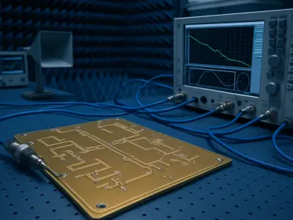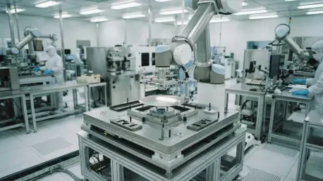

The transition to specialized BEOL memory could allow TSMC to achieve significantly higher bit density than traditional SRAM, which typically requires six transistors for every single bit cell. This shift represents a fundamental realignment of the semiconductor landscape as logic manufacturers attempt to solve the memory wall that currently limits artificial intelligence performance. In 2026, the industry is no longer characterized by a clear separation between compute and storage, but rather by an integrated approach aimed at reducing data latency. As the global chip supply chain bifurcates along regional lines, the pressure to innovate has reached a fever pitch. Traditional DRAM players face a dual threat from logic giants encroaching on their territory and the rapid, state-backed expansion of manufacturing capacity in mainland China. These dynamics are reshaping the economic foundations of the industry, forcing firms to re-evaluate their roadmaps to survive a period of intense competition.
Specialized Architecture: Bridging the Logic and Memory Divide
TSMC is pioneering a specialized memory architecture that integrates memory directly into the interconnect layers of logic chips through Back-End-of-Line (BEOL) processes. By utilizing Amorphous Oxide Semiconductor (AOS) channels and a one-transistor, one-capacitor (1T1C) configuration, the company is successfully building high-density memory arrays that sit atop delicate logic layers. This method employs a low-temperature fabrication cycle that avoids damaging the underlying transistors, effectively creating a multi-dimensional chip structure. Unlike traditional silicon-based solutions, this AOS-based memory addresses the persistent issue of standby leakage by providing an exceptionally low off-current. Such innovation allows for a dramatic increase in on-chip memory capacity, which is essential for the large language models and high-performance computing tasks that define the current technological era. This transition from horizontal layouts to integrated vertical stacks marks a new frontier in the quest for hardware efficiency.
Despite these technological advances, prominent industry veterans like Charles Kao remain deeply skeptical about the ability of logic manufacturers to dominate the specialized memory market. The fundamental argument is that the “high professional threshold” required for DRAM fabrication involves entirely different physical and electrical parameters than those found in high-speed logic production. While TSMC excels at producing the world’s most advanced processors, the structural integrity and retention characteristics of memory cells demand a different set of engineering competencies that have been refined by specialized firms over decades. Kao suggests that the technical hurdles associated with 3D DRAM mass production are so steep that even a logic powerhouse may struggle to achieve the necessary yields and cost structures. This perspective highlights a growing divide between those who believe in the convergence of manufacturing processes and those who maintain that logic and memory remain two distinct disciplines that require specialized focus.
Scale and Innovation: China’s Strategic Bid for Market Dominance
While the debate over technical integration continues, ChangXin Memory Technologies (CXMT) is executing an aggressive strategy based on massive physical expansion and volume production. Current projections indicate that CXMT is rapidly increasing its fabrication footprint, with multiple new facilities coming online to reach a combined capacity of approximately 600,000 wafers per month. This massive influx of production is designed to capture a significant portion of the global memory market, particularly in the general-purpose DRAM segment that powers consumer electronics and standard data centers. By 2028, the industry expects a flood of Chinese-made memory products that could disrupt the existing supply-demand equilibrium and challenge the pricing power of leaders. This expansion is not just about quantity; it is a move to establish a self-reliant semiconductor ecosystem that can withstand geopolitical pressures. The scale of this operation represents one of the most ambitious manufacturing ramps in the history of the memory industry.
The transition to more advanced architectures like the 4F² memory cell remains a central challenge for Chinese manufacturers as they attempt to move beyond sheer volume. This next-generation design stacks transistors and capacitors vertically, allowing for a significant reduction in the physical footprint of each cell and a bit density increase of up to 50 percent. However, the 4F² process is difficult to master due to persistent issues with electrical leakage and the complexity of creating reliable vertical capacitive structures. Observers note that while the theoretical advantages are clear, the practical implementation in a high-volume manufacturing environment is fraught with technical risks that could impede progress. If these hurdles remain unresolved, the strategy of massive expansion may lead to an oversupply of less efficient chips rather than a breakthrough in high-performance memory. The success of the 2026-2028 roadmap depends on whether these intricate engineering problems can be solved at scale without sacrificing manufacturing yield.
Strategic Outlook: Navigating the Global Semiconductor Ecosystem
The overarching driver behind these seismic shifts is the truly insatiable demand for advanced silicon fueled by the ongoing artificial intelligence revolution. As AI models become increasingly complex, the need for high-bandwidth, high-density memory has become the primary bottleneck in system performance. This environment has created a dual-track market where specialized, integrated solutions from companies like TSMC and high-volume commodity chips from firms like CXMT both find essential roles. For the logic sector, the goal is to bring memory as close to the processing core as possible to minimize data transit times. For the memory sector, the focus remains on scaling capacity to handle the vast datasets required for machine learning training. This bifurcation suggests that the market will continue to reward both architectural innovation and manufacturing scale, provided companies can navigate the shifting geopolitical landscape. The synergy between these tracks will likely dictate the next phase of compute capabilities and determine which firms lead the silicon economy.
The evolution of the memory market through 2026 demonstrated that traditional boundaries between manufacturing disciplines were increasingly porous but still presented significant engineering barriers. Stakeholders recognized that the move toward specialized BEOL integration offered a promising path for high-performance applications, even as skeptics pointed to the difficulty of mastering standalone DRAM physics. The aggressive expansion in China signaled a future where volume would compete directly with process sophistication, forcing global leaders to diversify their supply chains and accelerate their own R&D cycles. Industry analysts concluded that the successful navigation of this transition required a balanced approach that prioritized both localized vertical integration and the resolution of persistent leakage issues in cell designs. The lessons learned suggested that future success would depend on the ability to synchronize advanced packaging with novel materials. Firms were encouraged to invest in hybrid architectures that could bridge the gap between processing power and storage density.