
The relentless push for greater power density and efficiency in modern electronics has created a significant engineering challenge, where conventional printed circuit boards often become the bottleneck, unable to manage the intense electrical currents and resulting thermal stress. As devices across all sectors, from industrial machinery to renewable energy systems, demand more power in smaller footprints, the limitations of standard copper tracing have become increasingly apparent, leading to performance degradation and a higher risk of system failure. Responding to this critical industry need, Shenzhen-based manufacturer Victory PCB has announced a strategic focus on heavy copper PCB production, a specialized technology engineered to provide a robust and reliable foundation for the next generation of high-power electronic systems. This move signals a broader market shift towards solutions that prioritize durability and thermal management, addressing the fundamental physical constraints that have long governed power electronics design.
The Engineering Behind Enhanced Power Delivery
Defining a New Standard in Circuit Board Technology
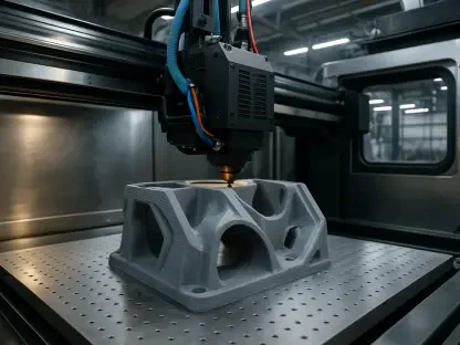
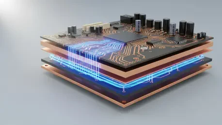
Heavy copper printed circuit boards represent a fundamental evolution in circuit design, engineered specifically for applications demanding superior current-carrying capacity and mechanical strength. These boards are formally defined as having copper thicknesses exceeding 3 ounces per square foot (oz/ft²) on their inner or outer layers, a significant increase over standard PCBs. The industry further classifies them into “heavy copper” for thicknesses ranging from 4 to 20 oz/ft² and “extreme copper” for robust applications requiring over 20 oz/ft², with some designs reaching up to 200 oz/ft². The manufacturing process for these specialized boards involves a sophisticated combination of precision etching and advanced plating techniques. This method is meticulously controlled to build up substantial copper thickness not only on the surface traces but also along the sidewalls of plated through-holes. The result is an exceptionally durable and reliable wiring platform capable of handling elevated currents without degradation, ensuring long-term stability and integrity even under continuous high-stress conditions.
This advanced construction offers designers significant architectural advantages, enabling the creation of more compact, efficient, and mechanically resilient electronic systems. By integrating high-current circuits directly onto the PCB, engineers can eliminate the need for bulky, separate bus bars or complex wiring harnesses that were traditionally required to manage significant power loads. This consolidation allows for a much higher circuit density, potentially reducing the overall layer count and physical size of the final product. The inherent strength of the thicker copper traces also enhances the board’s structural integrity, making it more resistant to thermal strain and mechanical stress. This simplified yet powerful structure streamlines the assembly process and reduces the number of potential failure points within the system. Consequently, designers are empowered to build sophisticated, high-power systems on a single, unified board that combines both power distribution and control circuitry, a feat that was previously impractical with conventional PCB technology.
Overcoming Thermal and Cost Barriers
One of the most critical advantages offered by heavy copper PCBs is their inherent capacity for superior thermal management, a crucial factor in the reliability and lifespan of high-power electronics. The substantial volume of copper in these boards acts as an excellent heat sink, leveraging the material’s high thermal conductivity to efficiently draw heat away from temperature-sensitive components like processors and power transistors. This passive heat dissipation significantly reduces the thermal strain on the entire circuit, preventing components from reaching critical temperatures that could lead to performance throttling or catastrophic failure. By effectively managing heat at the board level, designers can often reduce or eliminate the need for external cooling solutions such as fans or large heat sinks, further simplifying the overall system design and reducing its size, weight, and power consumption. This enhanced thermal endurance ensures consistent performance and dramatically improves the long-term reliability of the electronic assembly, particularly in harsh operating environments.
While the use of increased copper content might suggest a higher initial component cost, heavy copper PCBs frequently lead to a lower total cost of production and ownership when viewed holistically. The ability to integrate high-current pathways directly into the board architecture eliminates the expense associated with purchasing and installing separate components like thick-gauge wires, custom bus bars, and the associated connectors. This simplification translates directly into reduced material costs and significantly lower labor expenses during the assembly phase, as complex manual wiring is replaced by a more streamlined and automated process. Furthermore, the enhanced reliability and durability of these boards reduce the likelihood of field failures, minimizing warranty claims, repair costs, and the associated damage to brand reputation. By creating a more integrated, robust, and efficient design from the outset, heavy copper PCBs provide a cost-effective solution that optimizes not just performance but also the entire manufacturing and lifecycle anagement process.
Powering the Future Across Diverse Industries
Broad Applications in Demanding Sectors
The unique combination of high current capacity, exceptional thermal management, and mechanical robustness makes heavy copper PCBs indispensable across a wide range of demanding industries. In the realm of power electronics, they are essential components in power supplies for complex radar systems, high-efficiency power converters, and the control systems for solar panel manufacturing and nuclear power facilities. These applications depend on the boards’ ability to handle continuous, high-amperage loads reliably over extended service lifetimes. Industrial sectors also rely heavily on this technology for equipment such as heavy-duty welding machines and high-performance torque controls, where consistent power delivery is critical for operational safety and precision. Furthermore, safety and signal systems, including protection and overload relays and power line monitors, utilize heavy copper boards to ensure failsafe operation under fault conditions. The common thread uniting these diverse applications is the uncompromising need for consistent, reliable performance in harsh operating environments where failure is not an option.
The automotive industry, in particular, has become a major driver for the adoption of heavy copper PCB technology, fueled by the rapid transition toward vehicle electrification. In electric vehicles (EVs) and hybrid electric vehicles (HEHEVs), these boards are critical for managing the immense power that flows between the battery pack, inverters, and electric motors. They form the backbone of power distribution units, battery management systems (BMS), and onboard chargers, where managing both high currents and the resulting heat is paramount for safety and performance. The automotive environment is notoriously harsh, characterized by extreme temperature fluctuations, constant vibration, and exposure to moisture and corrosive agents. The inherent mechanical strength and thermal stability of heavy copper PCBs make them ideally suited to withstand these conditions, ensuring the long-term reliability of a vehicle’s most critical electronic systems. As automotive designs continue to integrate more powerful and complex electronics, the demand for these robust circuit solutions is projected to grow significantly from 2026 to 2028.
A Solidified Foundation for Power Electronics
The strategic pivot toward collaborative manufacturing has proven instrumental in accelerating the adoption and refinement of heavy copper technology for specialized applications. By fostering a close partnership between designers and manufacturers, companies were able to move complex concepts from initial design to full-scale production with greater efficiency and precision. This customer-centric model allowed for extensive customization, including the selection of specialized substrate materials, the development of intricate multilayer configurations, and the implementation of unique manufacturing processes tailored to specific performance requirements. This deep collaboration ensured that every board was engineered to meet exact design specifications and performance benchmarks. The resulting ability to reliably produce highly demanding boards with rapid turnaround times established heavy copper PCBs not as a niche product, but as a mainstream solution for any application where power, heat, and reliability were primary concerns. This approach has permanently altered the landscape of power electronics design.