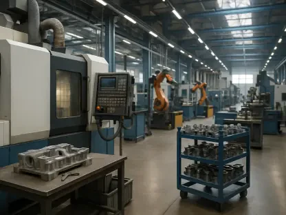

The semiconductor industry serves as the foundation of modern technology, underpinning the functionality of devices ranging from everyday smartphones to advanced supercomputers that drive innovation across sectors. As the demand for smaller, faster, and more energy-efficient chips continues to grow, manufacturers face unprecedented challenges in keeping pace with Moore’s Law—the principle that transistor counts on chips double roughly every two years. Traditional lithography, the critical process of etching intricate patterns onto silicon wafers to create microchips, struggles to meet the precision required for nanometer-scale features. Physical and economic barriers have pushed the industry to explore new frontiers, and artificial intelligence (AI) has emerged as a transformative force. By enhancing a cutting-edge technique known as inverse lithography technology (ILT), AI is redefining how semiconductors are designed and produced, offering solutions to problems once thought insurmountable. This exploration delves into the intersection of AI and semiconductor manufacturing, uncovering the profound impact of this technological synergy.
Breaking the Barriers of Conventional Lithography
The relentless pursuit of miniaturization in chip design has exposed the limitations of traditional lithography methods, which have long been the cornerstone of semiconductor production. For decades, techniques such as reducing exposure wavelengths or enhancing optical systems through increased numerical apertures provided the means to shrink feature sizes. However, these approaches are now hitting fundamental physical constraints and incurring costs that are no longer sustainable. As chip components approach scales measured in single-digit nanometers, even the slightest pattern deviation can result in significant performance failures, threatening the reliability of devices that power artificial intelligence systems, 5G networks, and beyond. The inability of conventional methods to deliver the required precision at such scales has created an urgent need for alternative strategies. This pressing demand has catalyzed the development of computational lithography, a field that employs algorithmic solutions to enhance accuracy, setting the stage for more advanced innovations to take center stage in the industry.
Computational lithography represents a paradigm shift, moving away from purely hardware-based solutions toward data-driven and algorithmic approaches that address the shortcomings of older techniques. Within this domain, inverse lithography technology (ILT) has emerged as a promising method to overcome the precision challenges faced by manufacturers. Yet, even as computational methods gain traction, the complexity of designing chips at unprecedented scales reveals additional hurdles, including the immense processing power required and the difficulty in translating designs into physical reality. These obstacles highlight a critical gap in the production process that must be bridged to sustain the rapid pace of technological advancement. Fortunately, the integration of artificial intelligence offers a pathway to navigate these challenges, enhancing ILT’s capabilities and providing a glimpse into a future where semiconductor manufacturing can keep up with ever-growing demands for performance and efficiency.
Unleashing Precision with Inverse Lithography Technology
Inverse lithography technology (ILT) marks a revolutionary departure from traditional lithography by reimagining the design process from the ground up. Rather than starting with a predetermined mask and predicting the resulting wafer pattern, ILT begins with the desired outcome on the wafer and works backward to determine the optimal mask configuration. This inverse approach relies on sophisticated mathematical frameworks and optimization algorithms to account for distortions and ensure unparalleled accuracy in pattern creation. By addressing deviations proactively, ILT achieves a level of precision that conventional methods struggle to match, making it an invaluable tool for crafting the intricate designs required for modern chips. This methodology is particularly crucial as feature sizes continue to shrink, demanding solutions that can handle the complexities of nanometer-scale production with consistency and reliability.
Despite its transformative potential, ILT is not without significant challenges that hinder its full adoption across the semiconductor industry. The computational intensity required to process these inverse calculations is immense, often necessitating vast resources and time, especially when applied to entire chip layouts. Additionally, the masks designed by ILT frequently feature curvilinear shapes that optimize pattern fidelity but pose substantial difficulties during manufacturing. Current fabrication tools are often ill-equipped to produce these complex geometries at scale, limiting ILT’s practical implementation. These barriers underscore the need for complementary technologies to enhance ILT’s feasibility for widespread use. As the industry seeks ways to overcome these obstacles, artificial intelligence has stepped in as a powerful ally, amplifying ILT’s strengths and addressing its limitations through innovative computational strategies that promise to redefine the production landscape.
Accelerating Innovation with AI-Driven Solutions
Artificial intelligence is breathing new life into inverse lithography technology by introducing levels of speed and efficiency previously unattainable through traditional computational methods. AI tools, particularly those leveraging deep learning, can simulate intricate lithographic processes—such as near-field diffraction and photoresist chemistry—at a fraction of the time required by conventional physics-based models. By training on extensive datasets of mask designs and corresponding wafer outcomes, these algorithms predict results with striking accuracy, significantly reducing the iterative cycles needed to perfect a design. This acceleration not only cuts down development timelines but also lowers the resource burden, enabling manufacturers to innovate more rapidly. The impact of this efficiency is evident in the ability to produce cutting-edge chips that meet the demands of emerging technologies, ensuring that the semiconductor industry remains at the forefront of progress.
Beyond enhancing speed, AI brings a nuanced capability to ILT by adeptly handling the minute details that define modern chip production. Hybrid models that integrate AI with established physical principles ensure that predictions remain grounded in real-world constraints while pushing the boundaries of precision. These models can address complex phenomena at scales that were once beyond reach, from extreme ultraviolet exposure dynamics to subtle resist effects, thereby improving the fidelity of wafer patterns. Such advancements are critical for crafting smaller, more power-efficient semiconductors that fuel advancements in diverse fields like machine learning and telecommunications. As AI continues to evolve, its synergy with ILT is unlocking new possibilities, demonstrating how data-driven insights can complement and enhance traditional engineering approaches to solve some of the most pressing challenges in chip design and manufacturing.
Navigating Challenges and Charting the Path Forward
Even with the remarkable advancements brought by AI-powered ILT, significant hurdles remain in scaling this technology to meet the full scope of industry needs. One of the primary obstacles lies in achieving full-chip optimization without sacrificing pattern consistency. Current practices often involve partitioning large chip layouts into smaller segments for processing, a method that introduces stitching errors at the boundaries and compromises overall design integrity. Moreover, while AI accelerates computations, it demands extensive labeled datasets for training and can sometimes lack transparency in its decision-making processes, raising concerns in industrial applications where reliability is paramount. Addressing these issues requires the development of more interpretable, physics-informed AI algorithms and automated workflows that minimize manual intervention, paving the way for ILT to become a scalable solution for complex, large-scale chip designs.
Another critical challenge centers on the physical production of the intricate mask geometries that ILT generates to optimize wafer patterns. Curvilinear shapes, while ideal for enhancing fidelity, are notoriously difficult to fabricate with existing tools like electron-beam direct writing, often necessitating simplifications that diminish the intended benefits. Emerging technologies such as multi-beam mask writing hold promise for improving throughput and resolution, but they are still in developmental stages and require further refinement to meet production demands. Overcoming these fabrication bottlenecks is essential to fully realizing ILT’s potential and ensuring that computational designs translate effectively into tangible products. Continued investment in both software enhancements and hardware innovations will be crucial to bridge this gap, enabling the seamless integration of advanced design techniques into mainstream manufacturing processes.
Building Tomorrow’s Semiconductor Landscape
Reflecting on the journey of semiconductor manufacturing, it’s clear that AI’s integration into inverse lithography technology marked a turning point in overcoming the constraints of traditional methods. The precision and efficiency brought by AI-driven ILT tackled the daunting task of shrinking feature sizes, ensuring that the industry kept pace with relentless technological demands. Hybrid models blending data-driven insights with physical accuracy, alongside accelerated computing, addressed critical design challenges that once seemed insurmountable. Though obstacles like full-chip optimization and complex mask fabrication persisted, the groundwork laid by these innovations proved transformative, reshaping how chips were conceptualized and produced for a digital era hungry for progress.
Looking ahead, the focus must shift to actionable advancements that build on this foundation. Prioritizing the development of transparent, physics-embedded AI models will enhance trust and adoption in industrial settings, while GPU acceleration can further slash computational timelines. Simultaneously, accelerating the maturation of multi-beam mask writing technology offers a viable path to streamline mask production. Collaborative efforts between software engineers and hardware developers will be vital to integrate multi-scale modeling, ensuring simulations account for both quantum and macroscopic effects. By fostering these synergies, the semiconductor industry can sustain its trajectory toward ever-smaller, more powerful chips, driving the next wave of innovation across artificial intelligence, telecommunications, and beyond.