
Kwame Zaire is a seasoned expert in industrial machinery and electronic production who has watched the manufacturing landscape evolve from rigid assembly lines to fluid, integrated ecosystems. By merging additive manufacturing, laser precision, and semiconductor bonding under one banner, he sees a path forward for North American companies to achieve unprecedented accuracy. This discussion explores the synergy of these platforms, the role of AI in monitoring reactive metal printing, and the breakthrough of cold-bonding dissimilar materials for future electronics.
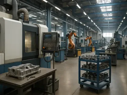
The shift to an Advanced Manufacturing Technologies division integrates metal additive, laser micromachining, and wafer bonding platforms. What operational advantages does this consolidation provide North American manufacturers, and how does combining these distinct technologies address the current gaps in high-precision production workflows?
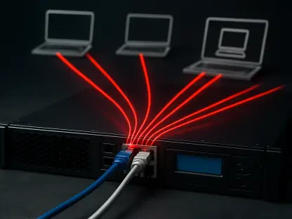
The shift to the Advanced Manufacturing Technologies division is about more than just a rebranding; it’s a strategic move to break down the silos between traditionally separate production stages. By integrating metal additive, laser micromachining, and wafer bonding, manufacturers gain a cohesive workflow where complex metal parts can be printed and then refined with micron-level precision. This consolidation allows North American shops to source multifaceted solutions from a single point of contact, ensuring that a component can transition from printing to specialized machining without data loss. It effectively closes the gap between raw additive output and the high-tolerance requirements of the semiconductor and aerospace industries.
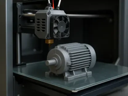
Large-scale metal 3D printing often faces significant hurdles with reactive materials and real-time quality monitoring. How does AI anomaly detection improve reliability in the LAMDA series, and what specific performance benefits does a local shield nozzle offer over traditional full inert gas enclosures?
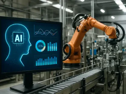
Reliability is the biggest hurdle in large-scale metal 3D printing, and the LAMDA series addresses this by acting as its own quality inspector through AI anomaly detection. This system provides real-time monitoring and instant feedback, allowing the machine to catch microscopic errors before they compromise a massive titanium structure. The real game-changer, however, is the local shield nozzle, which focuses an inert gas stream exactly where the melt pool occurs. This setup lets engineers print reactive materials without the physical and logistical headache of a massive, full-inert gas enclosure. It makes it possible to work on larger scales—up to the massive LAMDA 5000—without sacrificing safety or the purity of the material.
Drilling micro-holes down to 27 microns in silicon carbide and ceramics usually risks thermal distortion. How does a prism rotator facilitate ultra-high precision helical machining, and in what ways do flexible taper hole controls allow engineers to experiment with complex geometries like reverse-taper or hand-drum shapes?
When you are drilling holes as small as 27 microns in stubborn materials like silicon carbide, heat is your absolute enemy because it causes warping and structural fragility. The ABLASER uses a specialized prism rotator to execute helical machining, which distributes laser energy so precisely that thermal distortion is virtually non-existent. For engineers, this isn’t just about making holes; it’s about the freedom to design complex internal geometries, such as hand-drum or reverse-taper shapes, that were previously impossible to reach. Being able to toggle between straight and forward taper controls means we can now manufacture components for micro-electronics and medical devices that are both incredibly small and geometrically sophisticated.
Room-temperature wafer bonding eliminates thermal stress when joining dissimilar materials like gallium nitride and silicon. Could you describe the surface activation process within a high-vacuum environment and explain how this workflow scales from small-scale research to fully automated, high-volume 300 mm production?
The BOND MEISTER process is a fascinating departure from traditional methods because it relies on surface activation in a high-vacuum environment rather than intense, damaging heat. By cleaning and prepping the surfaces until they are ready to fuse at the atomic level, we can join materials like gallium nitride and silicon without the thermal stress that usually leads to cracking. This process is highly adaptable, starting with the MWB-04/06-R for research and prototyping where precision is paramount but volume is low. As a project scales, the workflow transitions to the fully automated MWB-08/12-ST, which handles 300 mm wafers in high-volume settings with a cassette-to-cassette operation that keeps throughput high and human error low.
What is your forecast for advanced manufacturing technologies?
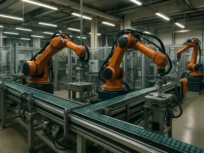
I forecast a future where “hybridization” is the standard rather than the exception, with machines capable of additive and subtractive tasks coexisting in a single automated loop. We are moving toward a reality where AI doesn’t just monitor the process but actively corrects the toolpath in milliseconds to guarantee zero-defect production. The ability to bond dissimilar materials at room temperature will also revolutionize the power electronics sector, enabling more efficient and compact electric vehicle components. Ultimately, the manufacturers who embrace these integrated, high-precision platforms will be the ones who lead the next industrial revolution.