
For the first time in nearly a decade, the monolithic dominance of the world’s most critical industry faces a genuine challenge from an American pioneer, as Intel’s successful transition of its 18A process node into high-volume manufacturing by the end of 2025 marks a seismic shift in the semiconductor landscape. This achievement is far more than a mere technological milestone; it represents the culmination of a grueling, high-stakes corporate turnaround, a strategic victory for United States’ industrial policy, and a fundamental realignment of the competitive dynamics powering everything from artificial intelligence to high-performance computing. Intel’s resurgence, built upon groundbreaking innovation and pivotal strategic partnerships, has effectively reset the terms of the global chip race, directly challenging the long-held manufacturing supremacy of its chief rival, Taiwan Semiconductor Manufacturing Company (TSMC), and ushering in a new era of intense competition at the bleeding edge of silicon technology.
A Leap in Foundational Technology
Intel’s remarkable resurgence is anchored by two transformative, industry-first technologies integrated into the 18A process, providing a tangible advantage in both performance and power efficiency. The first of these is RibbonFET, the company’s proprietary implementation of the Gate-All-Around (GAA) transistor architecture. As the successor to the long-standing FinFET design, RibbonFET surrounds the transistor channel with the gate on all four sides, a structural change that provides vastly superior electrostatic control. This innovation directly translates into significantly reduced power leakage and enhanced performance, allowing transistors to switch faster while consuming less energy. Intel has specifically optimized its RibbonFET design for the demanding, high-throughput workloads characteristic of modern AI accelerators and data center processors, establishing a new performance benchmark that competitors must now strive to match. This leap forward in transistor architecture is a core element of Intel’s claim to process leadership.
The second, and arguably more revolutionary, innovation is PowerVia, the industry’s first commercial deployment of backside power delivery. This groundbreaking technique fundamentally re-engineers the chip’s construction by relocating the intricate power delivery network from the top of the silicon wafer to the bottom, completely separating it from the signal interconnects. For years, designers have struggled with the “wiring mess” on top of the chip, where power and signal lines compete for limited space, leading to signal interference and voltage drop (IR drop) that can limit performance. By moving the power lines underneath, PowerVia solves this critical bottleneck, resulting in a cleaner signal environment and a more robust power supply to the transistors. Industry analysis suggests this separation yields a substantial 6% to 10% gain in clock frequency and a notable improvement in overall power efficiency, giving Intel 18A a distinct, albeit temporary, technological lead over TSMC’s competing N2 node, which will not incorporate similar backside power technology until its A16 node in 2026.
From Execution Woes to Manufacturing Excellence
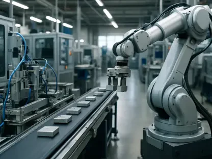
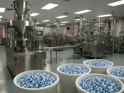
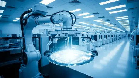
After years of well-documented manufacturing struggles and crippling delays that plagued its 10nm and 7nm nodes, Intel has convincingly demonstrated that it has fixed its execution engine. By late 2025, the yield rates for the 18A process have stabilized at an impressive 60%, a figure that proves the node is not only technologically advanced but also commercially viable for high-volume production. This stabilization is viewed by the research community as definitive proof of the company’s turnaround, silencing skeptics who doubted its ability to deliver on the ambitious “five nodes in four years” strategy. The first products to leverage this new process—the “Panther Lake” client CPUs and the “Clearwater Forest” Xeon server chips—are already reaching customers, serving as tangible evidence that Intel’s comeback is not just a roadmap promise but a market reality. This disciplined execution has been critical in restoring confidence among investors, partners, and customers.
While TSMC retains a numerical advantage in raw transistor density, Intel’s successful execution on 18A has made it a direct competitor for process leadership for the first time in nearly a decade. The combination of its lead in key technologies like backside power delivery and its proven ability to manufacture at scale has shattered the perception of an insurmountable gap between the two giants. This resurgence effectively ends TSMC’s de facto monopoly on the most advanced process nodes, introducing a new era of fierce competition that benefits the entire technology ecosystem. With two viable foundries at the leading edge, chip designers now have more options, fostering greater innovation and potentially mitigating the supply chain vulnerabilities that have characterized the industry in recent years. Intel’s return to form injects a much-needed dose of rivalry at the apex of semiconductor manufacturing.
The Rise of a Foundry Powerhouse
Intel’s comeback has fundamentally reshaped the foundry market, particularly for the high-value hardware that powers the artificial intelligence revolution. Operating as a quasi-independent subsidiary, Intel Foundry has successfully secured a roster of “anchor” customers who are strategically seeking to diversify their supply chains and reduce their singular reliance on Taiwan. Microsoft has publicly committed to using the 18A process for its next-generation Maia 2 AI accelerators, a significant design win that validates the performance of the node for cutting-edge AI workloads. Similarly, Amazon is leveraging the 18A node for its custom AI Fabric chips, driven by a desire to gain the “geographical resilience” offered by Intel’s advanced fabs located in the United States. These high-profile partnerships are not just commercial victories; they are strategic endorsements of Intel’s renewed manufacturing prowess and its role as a viable alternative to TSMC.
The renewed confidence in Intel’s manufacturing capabilities has reverberated throughout the industry, even prompting a strategic alliance with its long-time rival, NVIDIA. In a landmark move, NVIDIA made a $5 billion investment in Intel to co-develop custom x86 CPUs for data centers, signaling a profound shift in market dynamics. While NVIDIA will continue to use TSMC for its flagship GPUs, this partnership underscores a growing belief that Intel can reliably deliver leading-edge silicon. The emergence of a strong second foundry is also a significant boon for smaller AI startups and fabless design houses, which have often struggled to secure wafer allocation from a capacity-constrained TSMC. With Intel Foundry now a formidable player, these companies can expect relief from the severe supply constraints that have characterized the AI boom, fostering a more competitive and innovative marketplace for AI hardware.
The Geopolitical Stakes and Financial Realities
Intel’s 18A success story is deeply intertwined with a broader geopolitical narrative centered on U.S. industrial policy and the quest for technological sovereignty. The Department of Defense’s $3 billion “Secure Enclave” program formally establishes Intel as the sole domestic provider of sub-2nm chips for critical military and infrastructure applications, creating a protected market for its most advanced technology. This, combined with the U.S. government’s acquisition of a nearly 10% equity stake in the company, provides Intel with a significant financial and regulatory moat. This deliberate government backing positions Intel as a “National Champion,” tasked with the strategic objective of ending the nation’s reliance on foreign foundries for the most critical semiconductors and mitigating the profound supply chain risks associated with geopolitical tensions in the Taiwan Strait. Intel’s revival is thus a key component of a national strategy to onshore critical manufacturing capabilities.
However, this hard-won victory came at a substantial cost. A major corporate restructuring in early 2025, led by new CEO Lip-Bu Tan, was necessary to streamline operations and sharpen the company’s focus, resulting in a painful but necessary 20% reduction in its global workforce. Despite an impressive 80% surge in its stock price during 2025, which reflects renewed investor confidence, the financial reality is that Intel’s foundry business remains on a long and challenging road to recovery. Profitability for the foundry division is not expected until at least 2027, as the company continues to invest heavily in R&D and new fabrication facilities. The central question for Intel is now shifting away from technical capability—”Can they build it?”—and toward sustainable financial performance: “Can they scale it profitably?” The long-term success of its IDM 2.0 strategy will depend on answering this second question in the affirmative.
The Road Ahead and the Next Frontier
Intel did not rest on its laurels following the successful launch of 18A. The company had already prepared its next-generation Intel 14A node, a 1.4nm-class process, which was slated for risk production in late 2026 and was set to utilize the industry’s first High-NA EUV lithography machines. The next strategic frontier for market share became the lucrative mobile sector. While Intel had made significant inroads in data centers and PCs, it had yet to secure a major design win from Apple for its flagship iPhone processors, which remained firmly with TSMC. Advanced negotiations were reportedly underway for Apple to use Intel for some lower-end M-series chips by 2027, but winning the mobile crown required proving that 18A could meet the stringent thermal and battery-life demands of modern smartphones. The ultimate battleground, however, shifted towards advanced packaging. Intel’s Foveros and EMIB technologies were considered world-leading, and the company planned to leverage this advantage by integrating them with 18A to create massive, powerful “system-on-package” solutions tailored for the next wave of generative AI. This “war of attrition” with TSMC was fought not just at the transistor level but on the ability to integrate multiple chiplets into a single, cohesive, and powerful system.