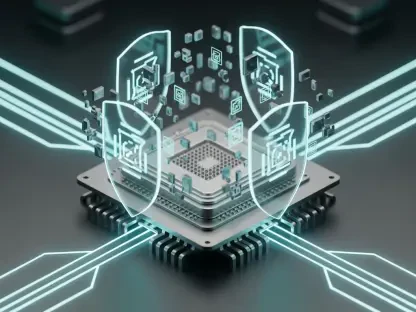

The global transition toward total silicon autonomy has reached a critical inflection point as traditional manufacturing constraints threaten to stall the rapid evolution of artificial intelligence. Terafab represents an ambitious strategic pivot toward vertical integration, established to bypass the bottlenecks of third-party dependencies. By rooting its operations in Austin, Texas, this initiative addresses the global AI compute shortage by shifting from a reliance on external foundries to a centralized, internal production model. This move is not merely about logistics; it is a fundamental reconfiguration of the tech supply chain.
Introduction to the Terafab Strategic Initiative
The project emerged from a clear discrepancy between current global semiconductor production and the massive requirements of next-generation AI projects. While industry giants have historically provided the backbone for silicon development, their expansion rates have struggled to keep pace with the accelerating demand for high-performance compute. By establishing internal facilities, the initiative seeks to secure a vertical supply chain that supports autonomous vehicles, humanoid robotics, and aerospace technology.
This shift toward localization reflects a broader desire for control over the hardware lifecycle. Relying on third-party manufacturers often introduces variables in lead times and prioritization that can hinder rapid innovation. By internalizing these processes in Texas, the project ensures that the production of essential components remains directly aligned with the specific hardware needs of its parent enterprises, fostering an environment where software and silicon evolve in tandem.
Technical Architecture and Key Components
Specialized Fabrication Facilities: The Power of Focus
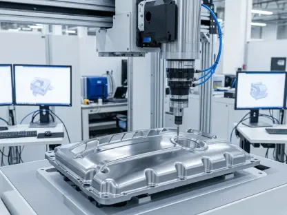
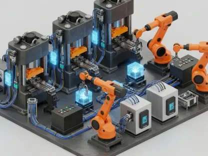
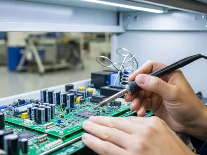
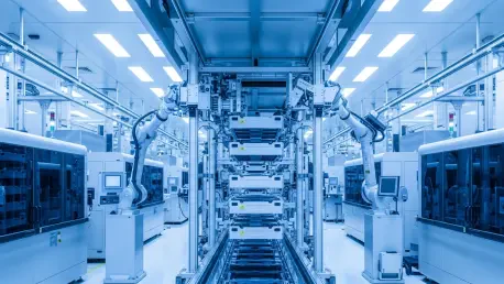
Efficiency in this model stems from extreme specialization within the two primary fabrication facilities. Unlike generic foundries that juggle hundreds of varied designs, these fabs focus on single-chip architectures, which drastically reduces the complexity of cleanroom operations. The movement of Front Opening Unified Pods (FOUPs) is optimized to follow the most direct paths, cutting down on idle time and mechanical wear. This narrow focus allows for a level of precision that traditional mega-fabs often struggle to maintain.
The Advanced Technology Fab: Flexibility in Production
The Advanced Technology Fab serves as the versatile heart of the Austin campus, housing equipment capable of rapid prototyping and diverse architectural shifts. While the specialized fabs handle high-volume output, this unit provides the necessary flexibility to pivot as new requirements emerge. This dual-track approach creates a buffer against technological stagnation, allowing for immediate iteration without disrupting the broader manufacturing flow of established silicon designs.
Current Trends and Industry Developments
Onshoring has become the defining strategy for high-tech enterprises seeking to mitigate geopolitical instability and logistical disruptions. The current market, nearing a trillion-dollar valuation, is increasingly driven by a desire for domestic self-sufficiency. Tech leaders are no longer content with being customers of the global semiconductor supply; they aim to become its primary architects. This shift represents a move from globalized interdependence toward localized resilience.
Furthermore, the gap between AI demand and physical compute output is forcing a rethink of industrial scaling. As the global market expands toward a projected $1.8 trillion by 2030, the ability to produce silicon internally becomes a massive competitive advantage. This trend suggests that the future of the tech economy will be defined by those who own the means of production rather than just the intellectual property of the designs.
Real-World Applications Across Industries
In practice, Terafab silicon powers everything from the neural networks in autonomous vehicles to the complex motor controls of humanoid robotics. The integration of specialized silicon is particularly vital for aerospace exploration, where radiation-hardened AI processors are required to withstand the harsh conditions of orbit. By controlling the production of these specific components, the initiative ensures that the hardware is perfectly tailored to the software, maximizing performance per watt in high-stakes environments.
Moreover, the deployment of these chips into large-scale satellite networks and large language models demonstrates the benefits of an integrated supply chain. Having direct access to custom silicon allows for faster training cycles and more efficient deployment of AI agents. This vertical integration ensures that every layer of the technology stack is optimized for the specific task at hand, reducing latency and increasing overall system reliability.
Challenges and Implementation Obstacles
Maintaining high yields in specialized environments remains a formidable technical hurdle. The industry is sensitive to material impurities and microscopic errors, which are often amplified in high-density localized models. Furthermore, the competition for specialized talent and raw materials creates constant pressure on operational costs. Regulatory frameworks also present obstacles as domestic manufacturing scales to meet unprecedented demand.
Logistical limitations inherent in a localized model also pose risks. While onshoring reduces international shipping risks, it creates a high-density point of failure if local infrastructure or resource availability is compromised. Balancing the benefits of proximity with the need for a resilient, diversified supply of raw materials is a delicate act that requires ongoing strategic adjustments and significant capital investment.
Future Outlook and Technological Trajectory
Looking ahead, the scalability of this model could set a new precedent for how large-scale corporate supply chains are structured. If successful, this project may pressure traditional leaders like TSMC and Samsung to rethink their own expansion rates and customer relations. The potential for total technological self-sufficiency offers a competitive edge that could redefine the pace of AI deployment over the next several years.
Future breakthroughs in chip architecture will likely focus on even deeper integration between processing units and specialized AI accelerators. The Terafab model is uniquely positioned to lead these developments because of its ability to test and implement new designs within its own ecosystem. This closed-loop development cycle could accelerate the transition toward truly autonomous systems that operate with unprecedented efficiency and intelligence.
Summary and Final Assessment
The Terafab project functioned as a decisive response to the systemic limitations of the global semiconductor market. It effectively bridged the gap between theoretical AI potential and the physical reality of hardware availability through its focus on localized, specialized manufacturing. While the risks of such a concentrated model were evident, the initiative established a blueprint for future industrial self-reliance. It transformed the way the tech industry approached the intersection of silicon production and autonomous software development. Moving forward, the industry must prioritize the cultivation of domestic talent and the stabilization of rare-earth material pipelines to ensure these facilities reach their full potential. This project proved that vertical integration is not just a luxury but a necessity for the next phase of global technological advancement.