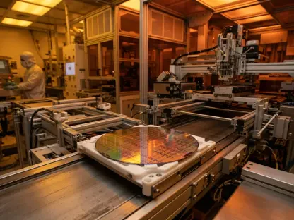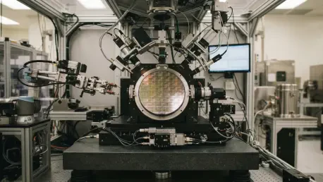

The silent heartbeat of every modern semiconductor fabrication facility is no longer just the speed of the etching tools or the purity of the chemicals, but the precision with which every microscopic feature is measured and validated. As the industry pushes deeper into the era of Gate-All-Around (GAA) field-effect transistors and multi-layer stacked nanosheets, the margin for error has effectively evaporated. In this high-stakes environment, metrology has transcended its traditional role as a simple verification step at the end of the line, becoming the primary engine of real-time process control and economic survival. The ability to resolve features at the atomic scale is currently the most significant bottleneck for manufacturing yield, as even a variation of a few nanometers can lead to catastrophic leakage or timing failures in high-performance chips. Without sophisticated measurement systems acting as the “eyes” of the factory, the complex three-dimensional designs required for modern artificial intelligence and data center processors would remain theoretical blueprints rather than physical realities. Consequently, the strategic importance of metrology has reached a point where it dictates the pace of innovation for the entire microelectronics supply chain.
The Role of Critical Dimension Measurement
Critical Dimension (CD) metrology stands as the foundational pillar of modern semiconductor manufacturing, focusing on the hyper-precise measurement of patterned features like line widths, contact hole diameters, and depth profiles. Because the electrical characteristics of a transistor are so closely tied to its physical dimensions, any deviation from the design specification can drastically alter the final performance or power efficiency of the component. To achieve the necessary resolution, manufacturers rely heavily on Critical Dimension Scanning Electron Microscopy (CD-SEM), which utilizes electron beams to visualize features far beyond the diffraction limit of visible light. Unlike the two-dimensional structures of the past, today’s features demand a level of precision where individual atoms must be accounted for during the inspection process. However, this level of scrutiny comes with its own set of challenges, as the high-energy electron beams used in SEM can inadvertently damage sensitive photoresists or cause material shrinkage during the measurement process. This creates a delicate balancing act where engineers must optimize beam energy and exposure time to obtain clear images without compromising the integrity of the wafer, ensuring that the measurement itself does not become a source of manufacturing defects.
To complement the high-resolution but potentially invasive nature of electron-beam tools, the industry increasingly utilizes optical metrology techniques such as scatterometry and spectroscopic ellipsometry. These methods are fundamentally non-destructive and offer significantly higher throughput, making them indispensable for monitoring wafers at various stages of the high-volume production line. Instead of creating a direct visual image of a feature, these tools analyze the complex patterns formed when light reflects and scatters off the wafer’s surface. By comparing these resulting optical signals against massive libraries of sophisticated mathematical models, engineers can infer the precise dimensions and material properties of the structures with remarkable accuracy. The success of this approach is entirely dependent on the quality of the underlying algorithms and the precision of the reference data used to calibrate the tools. As feature sizes continue to shrink, the mathematical models must become more complex to account for the subtle interactions of light at the nanoscale. This has led to a tighter integration between design-for-manufacturing (DFM) software and metrology systems, where the expected geometry of a chip is used to refine the optical models in real-time, allowing for faster and more reliable measurements across different production batches.
Managing Layer Alignment: The Challenge of Overlay
Since modern semiconductors are constructed through the meticulous deposition and patterning of dozens of different material layers, the alignment between these levels—technically known as overlay—is a critical factor for overall yield. If the patterns on a subsequent layer do not align perfectly with the structures already present on the wafer, the electrical connections between them will be severed or short-circuited, rendering the entire chip useless. Historically, this alignment was monitored using dedicated targets placed in the scribe lines, which are the narrow gaps between individual dies on a wafer. However, as the industry moves toward nodes that demand sub-nanometer overlay precision, these peripheral targets are no longer sufficient to represent the actual alignment within the dense functional areas of the chip. Localized distortions, often caused by the intense heat of annealing processes or the physical stress of thin-film depositions, can lead to subtle warping that varies across the surface of the wafer. This phenomenon means that while the edge of the wafer might appear perfectly aligned, the center could suffer from significant displacement, necessitating a more granular approach to measurement that looks directly at the functional components themselves.
To overcome these localized variations, there has been a definitive shift toward “on-device” metrology and the implementation of holistic alignment strategies that leverage data from multiple sources. By measuring the alignment of actual device features rather than just sacrificial targets, manufacturers gain a much more accurate view of the real-world conditions inside the chip. This data is fed back into the lithography scanners in a closed-loop system, allowing the machines to make instantaneous corrections to the wafer stage positioning and lens distortion for every individual exposure. This real-time compensation is essential for managing the cumulative stress that builds up as more layers are added, ensuring that even the most complex 3D structures remain perfectly synchronized. Furthermore, the integration of computational metrology allows for the prediction of potential alignment issues before they occur by analyzing historical data trends and correlating them with specific tool behaviors. This proactive approach to overlay management not only improves the final yield but also reduces the amount of time spent on manual inspections, allowing the fabrication facility to maintain high throughput without sacrificing the extreme precision required for the latest generation of processors.
Navigating Three-Dimensional Architectures
The transition from traditional planar transistors to three-dimensional architectures like Gate-All-Around (GAA) and stacked nanosheets has fundamentally disrupted the standard top-down metrology paradigm. In these advanced designs, the gate material fully encloses the channel, creating complex vertical structures and internal cavities that are effectively hidden from traditional surface-level imaging tools. This “hidden geometry” problem means that defects or dimensional errors occurring deep within the stack cannot be detected by standard scanning electron microscopes or optical tools, which only see the upper layers. To manage this complexity, the industry has turned to a strategy known as hybrid metrology, which combines the strengths of different measurement technologies to create a comprehensive three-dimensional model of the device. This approach involves correlating data from high-resolution, destructive techniques with faster, non-destructive tools to fill in the gaps in the factory’s visibility. Without this multi-modal view, it would be impossible to verify the uniformity of the nanosheet layers or the integrity of the gate-dielectric interfaces, which are the most critical components for ensuring the electrical performance of next-generation logic devices.
A central component of this hybrid strategy is the use of Transmission Electron Microscopy (TEM) to establish what is known as a “golden reference” for the production line. Although TEM provides the highest possible resolution, allowing engineers to see individual atomic planes, it is a slow and destructive process that requires physically cutting a thin slice out of a production wafer. Because of this, it cannot be used to inspect every wafer in a high-volume manufacturing environment; however, it is essential for calibrating the faster optical and SEM tools that are used on the main line. By comparing the detailed cross-sectional data from the TEM with the 2D signals generated by scatterometry tools, manufacturers can develop mathematical algorithms that accurately predict the internal 3D geometry based on the surface-level data. This allows for the non-destructive monitoring of buried features at production speeds, effectively turning the “blind” optical tools into sophisticated 3D sensors. This synergy between diverse measurement platforms is what enables the industry to maintain high yields even as the physical complexity of the chips increases, ensuring that the transition to 3D transistors does not lead to an unmanageable rise in manufacturing costs or defect rates.
Metrology in Advanced Packaging: The Rise of Chiplets
The scope of metrology is no longer confined to the front-end wafer fabrication process but is expanding rapidly into the “back-end” of advanced packaging and heterogeneous integration. As the industry moves toward “chiplets”—smaller, specialized dies that are bonded together to create massive, multi-functional systems—the requirements for surface preparation and alignment have become incredibly stringent. Technologies such as hybrid bonding, which eliminates traditional solder bumps in favor of direct copper-to-copper connections, require the bonding surfaces to be exceptionally flat and clean. Even a microscopic variation in topography or a slight recession of the copper bond pads can prevent a successful connection, leading to expensive failures at the final stages of the assembly process. Metrology tools must now be capable of evaluating surface flatness and bond pad alignment across large areas with nanometer-level precision, a task that requires a different set of technologies than those used for transistor patterning. This shift has placed a new emphasis on surface-sensitive measurements, where even the slightest atomic-level roughness can be the difference between a high-performance system and a pile of electronic scrap.
To address these challenges, manufacturers are increasingly deploying a combination of white-light interferometry and high-speed automated optical inspection (AOI) to ensure that every component is a “known good die” before it reaches the packaging stage. These tools are designed to detect a wide range of defects, from surface particles and scratches to subtle misalignments in the micro-bump arrays that connect the various chiplets. Because advanced packaging involves the integration of multiple expensive components, the cost of a single failure is much higher than in traditional manufacturing, making early detection an economic imperative. Modern AOI systems utilize advanced imaging sensors and specialized lighting to capture high-resolution data at incredible speeds, allowing them to inspect thousands of dies per hour without slowing down the production flow. By integrating this inspection data with the front-end fabrication records, engineers can trace specific packaging failures back to variations in the original wafer process, creating a unified data thread that spans the entire manufacturing lifecycle. This holistic view of quality control is essential for managing the complexity of modern heterogeneous systems, where the performance of the final product depends as much on the quality of the package as it does on the performance of the individual silicon dies.
Harnessing AI for Intelligent Process Control
As modern semiconductor fabs generate massive quantities of measurement data every single day, the industry’s focus has shifted from simple data acquisition to the generation of actionable intelligence through Artificial Intelligence (AI). The sheer volume of images produced by electron microscopes and the complex signals generated by optical tools are far beyond the capacity of human operators to analyze in real-time. To bridge this gap, machine learning algorithms are now being deployed to automate the interpretation of metrology data, identifying subtle patterns or anomalies that might indicate a drift in the manufacturing process. These AI systems can be trained to recognize the “fingerprints” of specific defects, such as a localized etching variation or a recurring lithography error, allowing the fab to take corrective action long before a batch of wafers is compromised. This move toward AI-assisted metrology is transforming the factory floor into a proactive environment where the measurement tools are not just flagging errors but are actively predicting potential issues based on historical trends and real-time sensor data from the manufacturing equipment.
Despite the clear advantages of speed and scale offered by AI, the semiconductor industry maintains a cautious and rigorous approach to the integration of these “black box” models. For an AI-driven metrology system to be truly effective, it must be continuously validated against physical reference standards and traceable international measurements to ensure its conclusions are grounded in physical reality. If a machine learning model is not properly calibrated, it can produce repeatable but inaccurate results, leading to a false sense of security that could result in thousands of defective chips. Therefore, the current trend is toward “explainable AI,” where the algorithms are designed to provide not just a pass-fail result but also the reasoning behind the classification, allowing human engineers to verify the findings. By linking metrology data with electrical test results and tool sensor logs, AI creates a closed-loop system that can automatically tune the manufacturing equipment to compensate for minor variations. This level of intelligent process control is the key to achieving high yields at the most advanced nodes, where the complexity of the manufacturing environment is simply too great for traditional statistical process control methods to handle effectively.
The Path Forward: Solving the Sampling Paradox
One of the most persistent challenges in semiconductor metrology is the “sampling paradox,” which describes the inherent conflict between the need for high-resolution accuracy and the requirement for high production throughput. In an ideal world, a manufacturer would measure every single transistor on every wafer to ensure perfect quality, but the time required for such an intensive inspection would bring the production line to a complete standstill. To resolve this tension, the industry is adopting “smart sampling” techniques that utilize historical data and predictive modeling to focus measurement efforts where they are most likely to yield significant results. By identifying specific areas of a wafer or particular stages of the process that are most prone to variation, metrology systems can concentrate their high-resolution capabilities on the highest-risk zones. This targeted approach allows the factory to maintain a high pace of production while still capturing the critical data needed to ensure long-term reliability. Furthermore, the use of virtual metrology—where process outcomes are predicted based on equipment sensor data rather than physical measurement—is being used to supplement physical inspections, providing a continuous stream of information that fills the gaps between physical sampling points.
The transition toward more intelligent and integrated measurement strategies enabled the microelectronics industry to overcome the diminishing returns of traditional inspection techniques. Manufacturers successfully moved away from isolated measurement steps, instead embracing a unified metrology framework that connected front-end fabrication, back-end packaging, and final electrical testing. Looking ahead, the focus must shift toward establishing standardized data formats and cross-industry protocols for sharing calibration data, as the complexity of multi-chiplet systems requires a level of transparency that traditional proprietary silos cannot support. The implementation of hybrid metrology and AI-driven analysis provided the necessary visibility to master the complexities of three-dimensional architectures, but future success will depend on the development of new reference materials that can withstand the demands of sub-nanometer nodes. These advancements in the “eyes” of the factory ultimately secured the economic viability of the most advanced nodes, proving that the science of measurement was just as critical to the digital economy as the designs of the processors themselves. By prioritizing traceability and data-driven intelligence, the industry established a resilient foundation for the continuous evolution of semiconductor technology, ensuring that future innovations would be built on a bedrock of precision and reliability.