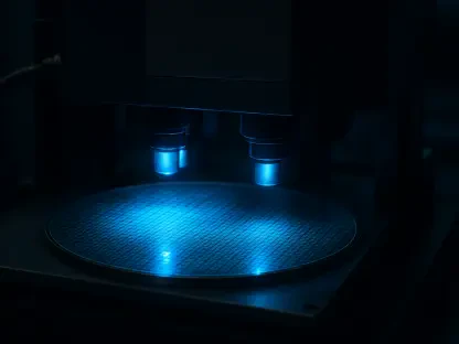

By substituting krypton for the standard argon gas during the sputtering process, researchers have successfully lowered the tantalum deposition threshold to just 200 degrees Celsius. This breakthrough addresses a persistent bottleneck in the fabrication of superconducting quantum processors, where the choice of material directly impacts the longevity of quantum states. Tantalum has emerged as a superior alternative to niobium due to its chemically inert surface, which naturally resists the formation of oxide layers that introduce decoherence. However, the requirement to heat substrates above 400 degrees Celsius to achieve the alpha phase has long threatened the structural integrity of delicate silicon components. By effectively halving the required thermal energy, this new sputtering technique preserves the microscopic architecture of the chip while ensuring the metal maintains its necessary electrical properties. This advancement simplifies the path toward creating stable, low-noise qubits that can perform complex calculations with much higher efficiency.
Atomic Momentum: The Physics of Heavy Ion Sputtering
The fundamental mechanism behind this improvement involves the manipulation of kinetic energy during the deposition of thin metal films. In traditional sputtering, argon gas serves as the medium to dislodge atoms from a target material, which then settle onto a substrate. While argon is abundant, its relatively low atomic mass limits the amount of momentum it can transfer to heavier elements like tantalum. By switching to krypton, which possesses a much larger atomic weight, researchers discovered that the ions strike the target with significantly higher impact force. This enhanced momentum is transferred to the tantalum atoms as they are ejected, providing them with enough energy to move across the substrate and settle into a highly ordered lattice. This increased mobility allows the atoms to find their optimal positions even in a cooler environment, bypassing the need for external heaters that often cause thermal expansion or hardware damage during the manufacturing process.
Beyond energy transfer, the use of krypton influences the structural phase of the deposited tantalum with precision. Tantalum can exist in two primary forms: the high-resistance beta phase and the low-resistance, superconducting alpha phase. For quantum computing applications, only the alpha phase is acceptable because it allows electrons to flow without resistance at cryogenic temperatures. In previous years, achieving this phase at lower temperatures was considered nearly impossible without introducing specialized seed layers or complex chemical buffers. The krypton-based method demonstrates that the physical energy of the incoming atoms alone can trigger the necessary phase transition. This development means that engineers can now produce high-performance superconducting films on a variety of materials, including those that would degrade under high-temperature conditions. It marks a shift from thermal-driven processes to momentum-driven ones, opening new doors for material design.
Interfacial Integrity: Eliminating Chemical Degradation
One of the primary beneficiaries of this lower temperature threshold is the interface between the metal and the underlying silicon substrate. When tantalum is deposited at temperatures exceeding 400 degrees Celsius, a destructive chemical reaction occurs at the boundary where the two materials meet. This reaction creates a thin layer of tantalum silicide, an unintended compound that acts as a source of electrical noise and energy loss. In the delicate environment of a quantum bit, even a few nanometers of this interfacial layer can cause a qubit to lose its quantum state, known as decoherence. By maintaining the environment at 200 degrees Celsius, the krypton sputtering process effectively prevents the diffusion of silicon atoms into the tantalum layer. This results in an atomically sharp boundary, ensuring that quantum signals remain protected from the disruptive influences of localized chemical impurities and structural defects that previously hindered performance.
The reduction in heat also mitigates internal stress within the thin films, which is critical for maintaining the stability of the entire quantum circuit. High-temperature deposition usually causes a mismatch in the thermal expansion coefficients between the metal film and the silicon wafer. As the chip cools down to the millikelvin range required for operation, this mismatch leads to mechanical strain, cracking, or peeling of the metal layers. Such physical defects are catastrophic for the reliability of high-density quantum processors. The krypton-based approach minimizes these stresses by narrowing the temperature gap between deposition and operation. Consequently, the resulting films exhibit higher electronic conductivity and a more uniform surface profile. This uniformity is essential for the fabrication of multi-layered structures, where every nanometer of variation can lead to significant fluctuations in the performance of the superconducting hardware, ensuring more consistent and reliable device behavior.
Industrial Scalability: Integration with Standard Manufacturing
The move toward a 200-degree process provided a major advantage for the commercial scaling of quantum technologies within existing semiconductor fabrication plants. Most modern high-volume manufacturing tools are optimized for temperatures in the range of 150 to 250 degrees Celsius, making the traditional 400-degree requirement for tantalum a difficult outlier. By aligning the tantalum sputtering process with industrial windows, manufacturers utilized current infrastructure to produce quantum chips without needing specialized high-heat vacuum chambers. This compatibility reduced the cost of production and accelerated the transition from laboratory prototypes to mass-produced quantum units. The ability to use standard photolithography and etching techniques alongside the krypton method ensured that the process remained repeatable and reliable. It established a sustainable path for the industry to move toward the same level of maturity and volume seen in the classical chip market, facilitating widespread adoption.
Looking forward, the successful implementation of krypton sputtering marked a turning point in the effort to modernize quantum hardware manufacturing. Researchers observed that the transition to heavier noble gases provided a viable solution to the thermal constraints that once limited the use of tantalum. This milestone demonstrated that the physical properties of the sputtering medium could be tuned to achieve specific material phases without relying on extreme heat. As a result, the technical barriers that separated the quantum laboratory from the commercial foundry were largely dismantled. Organizations involved in quantum development should now prioritize upgrading their physical vapor deposition systems to handle various heavy-ion gases. Standardizing these low-temperature deposition protocols across fabrication facilities will be essential for establishing a global supply chain. By focusing on these refined techniques, the technology community ensured that the next generation of quantum computers was built on a foundation of reliability.