
Semiconductor manufacturing has evolved into one of the most resource-intensive industrial processes on the planet, requiring an almost obsessive focus on the purity of every component that enters the cleanroom environment. As the industry pushes toward increasingly smaller transistor architectures, the traditional methods of water filtration are struggling to meet the rigorous demands of advanced lithography and wafer cleaning. This shift has placed a spotlight on the work of NSS Water, led by Björn Holmström, which advocates for a fundamental rethinking of how water is prepared for chip fabrication. Instead of relying on conventional multi-stage filtration that merely removes bulk contaminants, the company utilizes membrane distillation to produce water that is nearly identical to the theoretical ideal of pure ##O. This molecular-level precision is no longer just a laboratory curiosity but a critical requirement for maintaining high yields in a market where a single impurity can cause catastrophic failure across a silicon wafer.
The Evolution of Purity and Production Efficiency
Scientific Research: Scaling Precision for Industrial Yields
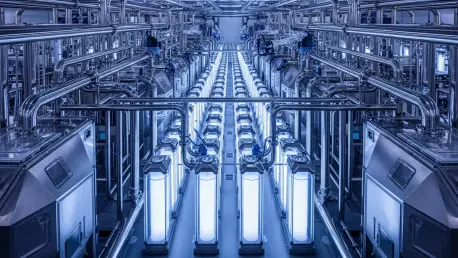
The technology underpinning this push for molecular purity emerged from an unlikely intersection of high-end electronics engineering and specialized research focused on zero-gravity environments. While attempting to measure the behavior of nanoparticles in space, Holmström identified a significant problem: the commercially available ultra-pure water used for scientific reference materials contained enough residual impurities to skew sensitive experimental results. This revelation prompted the development of a distillation process that isolates individual water molecules through a hydrophobic membrane, effectively leaving behind the salts and ions that bypass traditional filters. This approach represents a paradigm shift from trying to clean dirty water to specifically selecting only the molecules required for the process. By scaling this method for industrial use, it has become possible to provide semiconductor facilities with a level of consistency that was previously unattainable, bridging the gap between theoretical science and high-volume chip production.
Impact on Yield: Redefining Success in Chip Fabrication
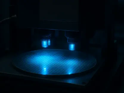
In the highly competitive world of fabrication, the economic viability of a facility is directly tied to its yield, which is the percentage of functional chips harvested from each silicon wafer. As the industry moves toward nodes of five nanometers and smaller, the margin for error is effectively non-existent, meaning that even a microscopic trace of metal or salt can bridge a circuit and destroy an entire batch. By integrating molecularly pure water into the cleaning stages of manufacturing, facilities can reduce the incidence of random defects that are often difficult to trace back to specific contaminants. This improvement in yield translates to billions of dollars in saved revenue and a significant reduction in the wasted energy and raw materials that occur when non-functional hardware must be discarded. The implementation of such high-purity standards ensures that the investment in cutting-edge lithography equipment is not undermined by the very fluids used to keep the production process running smoothly.
Strategic Implementation and Global Market Barriers
Aggressive Solvency: Managing Technical Interaction Challenges
One of the most persistent technical hurdles in deploying this technology is the inherent nature of ultra-pure water, which behaves as an incredibly aggressive solvent. Because pure ##O lacks minerals, it possesses a natural tendency to leach particles and gases from its immediate surroundings, including the pipes, storage tanks, and even the ambient air in a cleanroom. This aggressive characteristic means that traditional methods of laboratory testing are often flawed, as a water sample can become contaminated between the point of collection and the testing equipment. To counter this, the focus has shifted toward onsite, real-time monitoring and measurement at the exact point of use, ensuring that the water maintains its molecular integrity until the moment it touches the wafer surface. Maintaining this level of control requires a sophisticated infrastructure that treats water not just as a utility, but as a sensitive chemical reagent that must be managed with the same level of care as the photoresist chemicals or specialized gases.
Regional Market Dynamics: Navigating Global Adoption Hurdles
Despite the clear performance benefits, the global adoption of molecular water purification faces barriers rooted in the conservative nature of the semiconductor industry and regional market priorities. In Europe, a significant portion of semiconductor manufacturing is still geared toward the automotive sector, which often utilizes older, more robust processes that do not yet demand the extreme purity required for high-end processors. In contrast, the leading-edge fabrication hubs in South Korea, Taiwan, and the United States are facing immediate pressure to optimize their 2026-to-2028 production cycles for artificial intelligence and mobile hardware. These regions have become the primary testing grounds for membrane distillation technology because their thin margins for error make any increase in yield a high-priority objective. Navigating these regional differences requires a strategic approach that addresses the specific technical debt of older facilities while providing a clear roadmap for greenfield projects designed from the ground up to incorporate molecularly pure utilities.
Environmental Responsibility and the Corporate Roadmap
Driving Sustainability: Engineering for Resource Conservation
Beyond the immediate concerns of chip performance and factory profitability, the move toward molecular water purity offers a compelling narrative for improving the environmental footprint of the industry. Traditional cleaning processes often require massive volumes of water to ensure that contaminants are sufficiently diluted, but early research suggests that using higher-purity water can actually reduce the total volume needed. When the water is free of molecular noise, it performs its cleaning function more efficiently, allowing for shorter rinse cycles and a reduction in the reliance on harsh chemical surfactants and solvents. This shift aligns semiconductor production with broader global trends toward sustainable manufacturing, demonstrating that high-performance engineering can be a driver for resource conservation rather than a drain on local ecosystems. By focusing on the quality of the water at a molecular level, manufacturers are finding that they can achieve higher throughput while simultaneously lowering their environmental impact.
Strategic Implementation: Future-Proofing the Industrial Supply Chain
The strategic roadmap for the coming years emphasized the necessity of building deep technical partnerships between water purification specialists and fabrication plant managers. These collaborations proved essential for verifying the long-term stability of membrane distillation in high-volume environments and provided the data required to convince stakeholders of the technology’s reliability. Industry leaders prioritized the integration of modular purification units directly into the tool manifold to minimize the distance pure water traveled before use. Furthermore, manufacturers invested in advanced training for facility engineers to manage the unique challenges posed by aggressive solvents in ultra-clean environments. These steps ensured that the transition to molecular-level purity was not merely a theoretical upgrade but a practical shift that secured the supply chains for next-generation hardware. By treating water as a fundamental component of the silicon architecture itself, the industry successfully addressed the rising complexity of chip design with a focus on precision.