
Advanced packaging solutions are increasingly prioritized as the industry moves away from monolithic chip designs toward more versatile and complex chiplet architectures. This transition signifies a fundamental shift in how computing power is scaled, moving beyond the traditional shrinking of transistors to the strategic stacking of diverse functional components. As the limits of single-die manufacturing become more apparent, engineers are looking toward heterogeneous integration to maintain the performance gains expected in 2026 and beyond. This evolution, however, introduces unprecedented challenges in quality control and process reliability. The intricacy of interconnecting various chiplets requires a level of precision that was previously unnecessary in simpler architectures. Without the ability to inspect these internal structures with extreme accuracy, the risk of catastrophic yield loss increases significantly. Consequently, the industry is entering an era where metrology and inspection are no longer peripheral tasks but are central to the entire manufacturing strategy, necessitating tools that can see through solid silicon and identify flaws at the atomic scale.
Navigating Structural Complexity Through Advanced Inspection
Internal Interconnect Visualization and Reliability
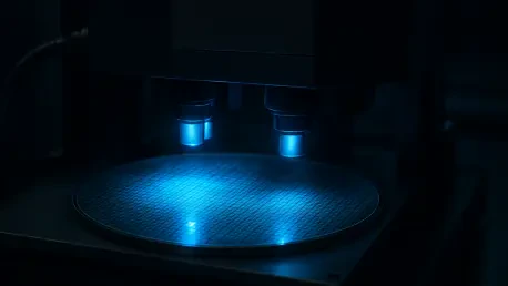
The rise of stacked die architectures has created a significant blind spot in traditional inspection methods, which were primarily designed for surface-level analysis. To address this, the ZEISS NLX system has emerged as a critical non-destructive inspection tool specifically optimized for 300-millimeter wafers. This technology utilizes advanced X-ray imaging capabilities to visualize the internal structures of chips, allowing manufacturers to examine the integrity of through-silicon vias and micro-bumps that reside deep within the finished assembly. By providing a clear view of these hidden layers without physically damaging the wafer, the system enables a more thorough validation of the vertical interconnect connections that are vital for the functionality of modern chiplet designs.
This capability is particularly important as the density of these connections continues to grow, making even the smallest misalignment or void a potential point of failure. The ability to identify such defects early in the production cycle ensures that resources are not wasted on processing faulty components, thereby improving overall factory efficiency. Furthermore, the implementation of such high-resolution imaging systems represents a shift toward predictive reliability in semiconductor manufacturing. By analyzing the structural data, engineers can develop a deeper understanding of how different materials and bonding processes behave under the thermal and mechanical stresses encountered during modern production, leading to more robust and reliable designs.
Implementing a Holistic Metrology Strategy
Mechanical stability has become a primary concern in modern fabrication as wafers undergo aggressive processing, including extreme thinning and multiple deposition cycles. These processes often lead to a phenomenon known as wafer bow, where internal stresses cause the silicon substrate to deform or warp. To manage this physical distortion, the ZEISS DUNE system provides a sophisticated solution by measuring and correcting wafer topography with extreme precision. This system is designed to handle the unique challenges of the 2026-2028 production roadmap, where maintaining a perfectly flat surface is essential for the successful bonding of multiple layers. It ensures that structural integrity is maintained throughout the entire fabrication sequence.
A comprehensive metrology framework was established to support these ambitious integration goals. This framework allowed manufacturers to navigate the transition to 3D systems by prioritizing holistic process control that bridged the gap between design and physical realization. Investing in these platforms early ensured that as margins for error shrank, production yields remained high, securing a competitive advantage in a market where precision became the ultimate currency. For organizations looking to lead, the primary recommendation was to adopt integrated metrology chains, which proved to be the definitive backbone of the supply chain and paved the way for the robust and high-performing microchips that power the digital world today.