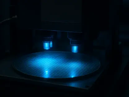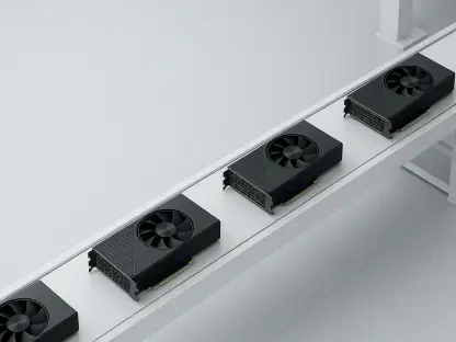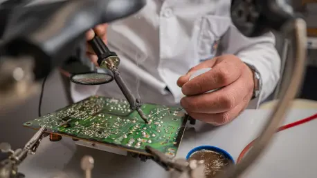

Japan remains a global leader in specialty chemical expertise, maintaining a 16.5% growth rate as it pursues advanced foundry capabilities. This regional strength provides a sturdy foundation for the global additive solder mask market, which is currently navigating a period of unprecedented transformation. As electronic devices become more sophisticated, the role of the solder mask has shifted from a simple protective layer to a critical dielectric component that ensures the integrity of high-frequency signals. The market, currently valued at approximately USD 114.1 million in 2026, is positioned for a remarkable journey toward a projected USD 520.0 million by 2036. This trajectory represents a compound annual growth rate of 14.8%, a figure that highlights the essential nature of these materials in the contemporary semiconductor landscape. This expansion is primarily fueled by the move toward extreme miniaturization in consumer gadgets and the stringent performance requirements of advanced semiconductor packaging. As the global digital infrastructure becomes increasingly reliant on high-speed computing and ubiquitous mobile connectivity, the demand for precision materials that can protect microscopic circuits from environmental hazards and electrical shorts has never been more pronounced, marking a new era in electronic manufacturing.
Financial Momentum: Analyzing the Absolute Growth Opportunity
The financial health of the additive solder mask industry is uniquely tied to high-value specialty chemicals rather than high-volume commodity goods. Even though the volume of material used in a single circuit board might seem negligible, these chemicals are vital for the success of multi-billion dollar semiconductor production lines. Between 2026 and 2036, the industry is expected to witness an absolute growth opportunity of nearly USD 389 million. This surge is less about simply manufacturing a higher quantity of boards and more about producing sophisticated, high-density substrates that require advanced masks. Investors and chemical manufacturers have recognized that the value lies in the precision of the formulation, which allows for finer resolution and better thermal stability. This focus on premium quality over quantity has fundamentally altered the investment landscape, drawing significant capital toward researchers who can push the boundaries of polymer science and light-sensitive resins.
This remarkably high growth rate of 14.8% for the materials sector signals a swift and decisive shift in how manufacturers construct modern electronics. This expansion is supported by massive investments in the global chip industry that have reached record levels this year. Programs like the CHIPS Act in the United States, along with similar multi-billion-dollar funding initiatives across Europe and Asia, are pumping capital directly into the supply chain. These government-backed efforts ensure that the infrastructure for advanced substrate manufacturing remains robust and capable of supporting next-generation technologies. By de-risking the development of new manufacturing facilities, these policies have encouraged material suppliers to invest in the specialized equipment needed to apply additive solder masks at scale. This influx of capital has created a self-reinforcing cycle where better materials lead to better chips, which in turn drives further demand for advanced chemical solutions.
Material Innovations: The Dominance of Photo-imageable Systems
Photo-imageable additives are currently the dominant material system in the market, holding a 42.0% share in the current year. Their widespread popularity stems from their unparalleled ability to create extremely precise openings for solder pads through a process known as photolithography. In the dense environment of modern electronics, where thousands of components are packed into an area smaller than a postage stamp, even a microscopic error in mask placement can ruin an entire production batch. Photo-imageable systems allow engineers to achieve the high level of detail necessary for modern high-density designs, making them the preferred choice for high-volume manufacturing facilities. These materials react to ultraviolet light, allowing for the creation of incredibly fine patterns that traditional mechanical application methods simply cannot replicate, thereby ensuring that every solder joint is perfectly isolated and protected from its neighbors.
Beyond simple precision, these advanced material systems are being engineered to meet the specific needs of integrated circuit substrates, which represent the most demanding application in the industry. These substrates act as the vital communication link between a tiny silicon chip and the larger printed circuit board. Because they involve microscopic copper structures that are highly sensitive to heat and moisture, the solder mask must be incredibly stable and chemically inert. As packaging moves toward complex three-dimensional designs, the mask must survive multiple rounds of intense heating during the assembly process without cracking or peeling. This has led to a rigorous testing environment where only the most durable chemical formulations can survive. The result is a specialized market where the performance of the photo-imageable additive directly dictates the overall reliability and lifespan of the final semiconductor product.
Industry Stakeholders: Dynamics of Substrate Manufacturers
Substrate makers are currently the primary drivers of demand, capturing approximately 44.0% of the market share as of 2026. These companies sit at the very top of the electronics manufacturing ladder, supplying critical components to the world’s largest and most influential semiconductor firms. Because their profit margins are directly dependent on their yield—specifically, how many chips they can successfully produce without defects—they are the fastest to adopt any technology that promises to improve reliability. By integrating advanced additive masks into their production lines, they can ensure that their products meet the incredibly strict standards of the tech giants they serve. This demand from the top of the supply chain trickles down, forcing material suppliers to constantly innovate and provide masks that can handle smaller pitches and higher electrical frequencies.
In addition to dedicated substrate makers, electronics fabricators and assembly providers are also shifting their focus toward these advanced materials to stay competitive. As the industry evolves, companies are looking for ways to offer more complete, end-to-end services, moving into specialized processing that was once the exclusive domain of niche boutique shops. This trend toward vertical integration means that more players in the supply chain are now actively searching for high-performance solder masks to differentiate their service offerings. By providing a superior coating, a fabricator can offer higher reliability and better thermal management to their clients, which is a significant selling point in the current market. This broadening of the user base is contributing to the overall growth of the market, as the technology moves from a specialized luxury to a standard requirement for any high-quality electronics production.
Miniaturization Trends: Precision in High-Density Environments
The trend toward extreme miniaturization remains the single biggest factor pushing the additive solder mask market forward. As consumer devices like smartphones, smartwatches, and medical wearables become thinner and more powerful, the physical space between electrical paths on a circuit board continues to shrink. Traditional solder masks often fail at these tiny scales, as the mechanical application methods are not precise enough to prevent the material from bleeding into areas where it is not wanted. Additive masks, however, provide the resolution needed to maintain tiny “dams” of insulation between solder points. This precision is essential for preventing electrical failures and short circuits in the incredibly dense environments of modern hardware. Without the ability to place a protective layer with micron-level accuracy, the development of the next generation of compact, high-performance gadgets would be impossible.
This demand for precision is also driven by the increasing complexity of high-density interconnect boards, which are used in everything from high-speed servers to autonomous vehicle controllers. These boards feature multiple layers of circuitry that must be perfectly aligned and insulated. Additive solder masks play a crucial role here, as they can be applied in thin, uniform layers that do not interfere with the overall thickness or weight of the device. Furthermore, the ability to use digital application methods like inkjet printing allows for on-the-fly adjustments to the mask pattern, accommodating slight variations in the board’s dimensions. This flexibility is a game-changer for manufacturers who need to maintain high yields while working with increasingly tight tolerances. As the industry pushes toward even smaller nodes, the reliance on additive technology will only intensify, making it a permanent fixture in the manufacturing toolkit.
Research and Policy: The Impact of Global Investment
Government research and public policy have become significant catalysts for innovation in the chemical supply chain. Currently, public funding is being used strategically to bridge the gap between initial laboratory research and high-volume factory production. When governments provide substantial grants for advanced packaging and semiconductor research, it significantly lowers the financial risk for material suppliers to develop and test entirely new chemical formulas. This creates a much safer environment for companies to experiment with cutting-edge chemistry that can handle the extreme needs of next-generation computing. These policies are not just about manufacturing; they are about securing a technological advantage in the materials science that underpins the entire electronics industry, ensuring that a nation’s supply chain is resilient and self-sufficient.
Furthermore, the alignment of public policy with industrial needs has led to the creation of specialized research hubs where chemical engineers and semiconductor designers work side-by-side. This collaboration ensures that new solder masks are developed with a deep understanding of the future requirements of chip architecture. For instance, as AI chips become more heat-intensive, research funded by these government initiatives is focusing on masks with superior thermal conductivity and resistance to high-voltage breakdown. This proactive approach to material development ensures that when a new chip design is ready for mass production, the necessary protective materials already exist and have been fully validated. This synchronization between policy, research, and industry is a primary driver of the rapid growth we are seeing in the market today, as it accelerates the time-to-market for revolutionary electronic products.
Functional Reliability: Performance Needs and Green Chemistry
In the high-stakes world of semiconductor manufacturing, even a fractional increase in the percentage of working parts can translate into millions of dollars in additional profit. Modern solder masks are no longer viewed as simple passive covers; they are now considered functional layers that actively contribute to the performance and lifespan of a device. Advanced additive masks are specifically designed to improve the way solder sticks to the board and to significantly reduce the release of trapped gases during the high-heat assembly process, a phenomenon known as outgassing. These technical improvements directly lead to fewer hidden defects and more reliable products for the end consumer. By ensuring that the solder joints remain stable over years of use, these masks help companies reduce warranty claims and build a reputation for high-quality, durable hardware.
At the same time, environmental regulations are forcing the industry to fundamentally change its chemical compositions. New laws regarding hazardous substances are requiring manufacturers to move away from traditional solvents and towards more sustainable alternatives. Companies that can provide “green” solder masks that meet these strict environmental standards without sacrificing performance are seeing a massive surge in interest from global brands. This shift toward sustainable chemistry is being driven by both government mandates and the corporate responsibility goals of major electronics companies that are eager to reduce their overall environmental footprint. As a result, the market is seeing a wave of innovation in water-based and low-VOC formulations that are safer for workers and the environment, proving that high performance and ecological responsibility can go hand-in-hand in the modern era.
Operational Hurdles: Qualification Cycles and Uniformity Challenges
Despite the robust growth, there are significant hurdles that companies must overcome to succeed in this market, most notably the long and expensive qualification cycles for new materials. A manufacturer cannot simply switch to a new solder mask overnight; the material must pass months of extreme stress testing to ensure it will not fail under real-world conditions. These tests involve thousands of hours of thermal cycling, humidity exposure, and electrical bias testing. For many smaller factories or start-up chemical firms, the cost and time required for this exhaustive validation are often too high to manage. This creates a market environment where established companies with a long track record of reliability have a significant competitive advantage, as customers are often very reluctant to switch away from a proven and certified product that they know will work.
Another major technical challenge involves the difficulty of maintaining perfect thickness uniformity across large manufacturing panels. Even when using the most advanced application methods, such as high-speed inkjet printing, keeping the coating consistent to within a few microns is a complex task. Any variation in the thickness of the mask can cause serious problems, such as interfering with high-speed signals or creating uneven pressure when chips are attached to the board. Achieving perfect uniformity at high production speeds is one of the primary goals for equipment and material designers today. This requires a deep understanding of fluid dynamics and real-time sensor technology to adjust the application process on the fly. Companies that can solve these uniformity issues while maintaining high throughput are the ones that will ultimately capture the largest share of the growing additive market.
Regional Leadership: The Centrality of the East Asian Corridor
The manufacturing heart of the additive solder mask industry is firmly located in East Asia, where a cluster of powerful economies dominates the supply chain. Japan continues to lead the way in chemical expertise, with its companies setting the global standard for the high-performance resins and photo-initiators used in these masks. The Japanese government is also heavily investing in local production facilities to ensure it maintains its competitive edge in the face of rising global competition. Meanwhile, China is growing at a rapid pace due to the massive scale of its domestic electronics sector and its clear national goal of becoming entirely self-sufficient in all aspects of semiconductor technology. This internal demand is driving Chinese firms to develop their own high-end solder mask formulations to reduce their reliance on foreign suppliers.
South Korea and Taiwan are equally vital to the future of the market, each bringing their own specialized strengths to the table. South Korea’s market growth is intimately tied to its massive memory chip industry, which requires specialized solder masks capable of handling the extreme heat generated in AI data centers. Taiwan remains the world’s central hub for foundry services, where the most advanced chips in existence are manufactured. The incredibly close working relationship between Taiwanese chip factories and their material suppliers ensures a constant and predictable demand for the most sophisticated additive solder mask technologies available. This regional concentration of expertise and manufacturing power means that any major developments in the market are likely to originate from this East Asian corridor, as these nations continue to push the boundaries of what is possible in electronics.
Western Specialization: High-End Research and Industrial Applications
In the United States, the focus of the additive solder mask market has shifted toward high-end research and development for strategic industries such as aerospace, defense, and medical technology. While high-volume consumer manufacturing moved overseas years ago, the U.S. is currently using the CHIPS Act to rebuild and strengthen its advanced packaging capabilities on domestic soil. This focus on high-reliability, low-volume production creates a niche but very profitable market for advanced solder mask suppliers who can meet stringent military-grade specifications. These applications require materials that can survive the vacuum of space or the extreme vibrations of a jet engine, necessitating a level of chemical engineering that goes far beyond what is required for standard consumer electronics. This specialized demand ensures that the U.S. remains a vital player in the high-end materials market.
Germany serves as the primary center for the electronics industry in Europe, with a particular focus on the automotive and industrial sectors. With European governments supporting the construction of new semiconductor plants across the continent, Germany is positioning itself as a global leader in power electronics. The rapidly growing electric vehicle market, in particular, requires durable and high-voltage resistant solder masks that can survive the harsh conditions of an automotive engine compartment. This industrial demand ensures that European material science continues to play a major role in the global market, as researchers focus on developing masks that can handle the unique challenges of high-power applications. By catering to these specialized industrial needs, Western markets are carving out a secure and essential space in the global additive solder mask landscape, focusing on quality and reliability over sheer volume.
Strategic Evolution: The Transition to Functional Components
The industry successfully navigated the transition from traditional subtractive methods to advanced additive processes by prioritizing R&D in specialty resins and digital ink formulations. Major stakeholders recognized that the path to a half-billion-dollar valuation was paved with strategic investments in environmental sustainability and precision inkjet technologies that offered a clear alternative to legacy systems. They established new benchmarks for material reliability and chemical stability, which ensured that the next generation of 5G and AI hardware could function reliably under extreme thermal and electrical stress. This collaborative approach between chemical suppliers and substrate makers ultimately redefined the boundaries of what was possible in microelectronics assembly, moving the solder mask from a simple protective coating to a highly engineered functional component.
Looking back at the progress made, it was clear that the adoption of additive solder masks was driven by a fundamental need for precision that traditional methods could no longer provide. The industry moved toward a future where every drop of material was utilized efficiently, and every circuit was protected by a layer of chemistry designed for its specific electrical environment. For stakeholders moving forward, the focus remained on maintaining this momentum by further integrating digital manufacturing techniques and exploring new bio-based materials that could further reduce the industry’s environmental impact. This journey reflected a broader trend in technology where the smallest, most overlooked layers were recognized as the essential foundation for the most advanced computing systems in the world, ensuring a robust and innovative future for the entire electronics ecosystem.