
Traditional Design Rule Checking often involves exhaustive manual debugging cycles that delay the tapeout process for high-performance computing hardware and mobile processors. This bottleneck is intensified by the shrinking physical dimensions of transistor gates, where even a microscopic misalignment can render an entire wafer useless. The semiconductor industry is currently navigating a period of unprecedented complexity as chip architectures move toward smaller process nodes and intricate three-dimensional structures. To address the resulting engineering bottlenecks, industry leaders like Siemens and TSMC have expanded their collaboration to integrate advanced artificial intelligence agents into the electronic design automation ecosystem. This initiative aims to streamline the verification and implementation of next-generation integrated circuits, particularly at the most advanced manufacturing nodes. By leveraging AI, engineers can manage the staggering density of modern transistors while maintaining precision.
Orchestrating Design with Intelligent Agent Systems
Autonomous Debugging: The Shift Toward Intelligent Reasoning
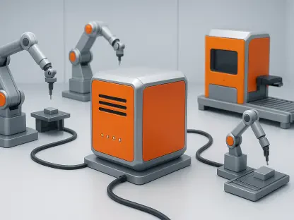
The most transformative aspect of this technological shift is the deployment of specialized AI systems that automate multi-step tasks across different software platforms. Traditionally, design verification has been a labor-intensive manual process where engineers must identify and resolve manufacturing violations before a chip reaches the final production stage. These new AI agents are designed to coordinate activities across various tools, allowing the system to not only identify errors but also suggest and implement fixes autonomously. This agentic approach shifts the focus from simple automation to intelligent reasoning, where the software evaluates intermediate results to ensure the chip layout remains compliant with strict manufacturing requirements. By utilizing high-performance AI technologies, Siemens has introduced a workflow that evaluates complex design data in real time, reducing the time engineers spend on repetitive debugging tasks.
Structural Integrity: Managing the Complexity of 3D Stacking
As the physical limits of traditional planar chips are reached, the industry is increasingly turning to 3D chip packaging, which allows for the stacking of multiple dies within a single package. This complexity introduces significant challenges regarding signal integrity and heat dissipation that manual methods can no longer effectively manage. AI-driven verification tools now support multi-machine processing to verify inter-chiplet connections, ensuring that the stacked components function harmoniously. By automating the routing configurations between separate dies, these intelligent systems help engineers overcome the spatial constraints inherent in advanced three-dimensional designs. Specifically, tools like Calibre 3DStack Advanced have been optimized to handle the intricate verification of inter-chiplet antennas, particularly for designs utilizing system-on-integrated-chips technology. This ensures that as die-to-die communication becomes more frequent, the electrical paths remain robust.
Ensuring Reliability and Precision at the Sub-Nanometer Level
Thermal Dynamics: Predicting Heat Flow in Vertical Architectures
Thermal management has become a critical factor in chip performance, as heat generated by stacked components can compromise the lifespan of a device. Modern AI-integrated tools are now certified for both static and transient thermal analysis, providing high-fidelity simulations that predict how heat will move through complex structures. Furthermore, specialized software ensures power integrity by performing transistor-level voltage-drop and electromigration analysis. These capabilities are vital for maintaining power efficiency and operational stability in high-performance computing environments where even minor fluctuations can lead to system failure. The certification of tools like Calibre 3DThermal for the latest A16 process ensures that engineers can accurately model thermal gradients across multiple layers of silicon. This level of precision prevents localized hotspots from developing, which is essential for the reliability of mobile processors and data center hardware.
Node Certification: Validating Performance for A14 and A16
A critical component of integrating AI agents is the formal certification of verification tools for the most advanced process nodes. This certification ensures that the software provides the extreme accuracy required for manufacturing at the smallest scales, such as the A14 and A16 nodes. These tools cover a comprehensive range of checks, from physical layout comparisons to electrical reliability assessments. By achieving high-fidelity simulation accuracy for analog, radio-frequency, and memory designs, these AI-enhanced platforms provide a reliable foundation for the mass production of next-generation hardware. Specifically, the Solido Simulation Suite and mPower software have been validated for transistor-level voltage-drop and electromigration analysis. This rigorous testing phase ensures that chips can maintain operational stability even under the intense workloads typical of artificial intelligence and high-performance computing applications.
Future Implementation: Silicon Photonics and Technical Expertise
The integration of silicon photonics and the launch of specialized educational initiatives marked a turning point for the global semiconductor workforce. Engineers utilized AI-driven tools to design photonic engines that integrated optical communication directly into silicon, facilitating faster data transfer for next-generation networks. Meanwhile, the expansion of the Xcelerator Academy provided design partners with the hands-on implementation workflows necessary to master advanced manufacturing nodes from 2026 to 2028. This comprehensive approach ensured that technological progress was matched by human expertise, allowing firms to navigate the complexities of 3D-integrated circuits. Moving forward, the move toward a closed-loop design environment proved essential for maintaining the pace of innovation. Stakeholders who adopted these agentic systems successfully shortened their development cycles and optimized their hardware for the power-hungry demands of the modern digital landscape.