
The landscape of silicon production has reached a point where traditional boundaries no longer apply to the high-stakes world of advanced computing. The rapid surge in artificial intelligence computing requirements is dismantling the traditional linear division of labor that once defined the global semiconductor industry. For years, the sector relied on a predictable, sequential flow where fabless designers created the blueprints, foundries printed the circuits on wafers, and assembly firms handled the final protection and testing. This legacy model functioned effectively when transistor shrinkage was the primary driver of progress. However, as we move through 2026, the industry is seeing a total collapse of these silos. The complexity of modern AI accelerators requires a simultaneous, rather than sequential, approach to manufacturing. Today, the design of a chip is inextricably linked to the specific capabilities of the packaging house and the memory supplier, forcing a degree of integration that was previously unnecessary. This shift is not merely a technical adjustment but a fundamental structural transformation that is redefining how value is created and captured across the global electronics supply chain, turning a linear chain into a dense, interdependent web.
Technological Complexity: The Rise of the Packaging Bottleneck
The current generation of AI hardware, exemplified by massive multi-die architectures, has pushed the limits of what a single piece of silicon can achieve. These designs often integrate two or more high-performance dies into a single unit, connected by high-speed interconnects that allow them to function as a unified processor. This evolution means that the performance of the system is no longer dictated solely by the number of transistors packed onto a wafer; it is now defined by how effectively those dies can communicate with each other and with external memory. Consequently, the focus of innovation has shifted from the front-end fabrication of logic gates to the back-end complexity of integration. When a single component, such as an organic substrate or a specific micro-bump material, faces a shortage, the entire production of high-end AI chips comes to a standstill. This transition has effectively moved the industry from being wafer-constrained to being packaging-constrained, where the ability to assemble complex systems is the primary gatekeeper for market availability.
Market dynamics in 2026 reflect this shift, with global foundry revenues projected to climb toward $220 billion as demand for advanced nodes remains at historic highs. This growth is being driven not just by traditional semiconductor giants but by a new wave of “hyperscalers” like Google, Meta, and Amazon, who are now developing their own proprietary silicon to optimize their data centers. Because these custom chips utilize the most advanced 3nm and 2nm processes, manufacturing capacity is consistently sold out years in advance. This extreme demand environment forces a complete rethink of resource allocation across the supply chain. Manufacturers are no longer simply filling orders; they are orchestrating a complex ecosystem where the timing of wafer output must perfectly align with the availability of specialized high-bandwidth memory and advanced 2.5D packaging capacity. The resulting pressure has turned the supply chain into a high-precision logistical machine where any minor delay in one segment can result in billions of dollars in lost revenue for the end customer.
Strategic Investment: The New Role of Fabless Designers
In this environment, the traditional “Fabless” model has evolved into a much more capital-intensive and hands-on endeavor. Leading chip designers can no longer afford to simply hand over a design and wait for the finished product; they must now act as strategic investors and co-managers of their suppliers’ facilities. To ensure supply chain resilience and guaranteed access to limited production lines, major design firms are engaging in massive capital expenditures on behalf of their partners. This includes using long-term agreements and multi-billion-dollar advance payments to fund the construction of new assembly plants and testing facilities. For instance, the recent expansion of testing capacity in the United States and South Korea has been largely financed by the very companies that will use those services, effectively locking in dedicated production slots for several years. This shift turns the relationship between designer and manufacturer into a deep financial partnership where both parties share the risks and rewards of physical infrastructure expansion.
This trend toward “total supply chain control” is creating a significant polarization within the semiconductor industry. Companies with vast cash reserves are able to “buy” a guaranteed future by funding the development of new substrate technologies and specialized testing equipment. For example, some designers have provided over a billion dollars in advance payments to ensure that specialized substrate manufacturers can expand their capacity by 250% to meet upcoming demand. While this secures the production roadmap for the industry’s leaders, it creates a challenging landscape for smaller firms and startups that lack the capital to secure similar priority. These smaller players may find themselves sidelined, unable to compete for the scarce advanced manufacturing slots that have been prepaid by larger rivals. This consolidation of power suggests that the ability to manage a massive capital budget is now just as important as the ability to design a high-performance chip, marking a permanent departure from the asset-light strategies of the past.
Co-Opetition: Redefining Rivalry in the AI Era
A striking feature of the semiconductor landscape in 2026 is the blurring of competitive lines, a phenomenon known as “co-opetition” where rivals become essential service providers for one another. In an era where no single company can meet the massive demand for AI infrastructure alone, enterprises that were once fierce competitors are now forming strategic alliances to maximize total output. For instance, we see major foundries acting as original equipment manufacturers for their competitors’ specific components. In one landmark $2 billion agreement, a secondary foundry has begun supplying silicon interposers for a primary competitor’s advanced packaging ecosystem. This allows the primary foundry to offload lower-margin production while focusing its internal capacity on core high-end processes. By collaborating in this manner, both companies maximize their revenue and ensure that the global market for AI accelerators remains supplied, even if it means helping a direct rival bring their products to market more efficiently.
This collaborative spirit is particularly evident in the production of customized memory solutions, such as the latest iterations of high-bandwidth memory. The production of these critical components often requires a tripartite effort between a memory specialist, a logic foundry, and a systems designer. A single high-end memory stack might feature a logic base produced on a cutting-edge 3nm process by one company, integrated with memory layers manufactured by another. This modular approach prioritizes speed to market and technical excellence over traditional brand rivalry. Industry leaders have recognized that the complexity of the AI hardware stack is too great for any one entity to dominate every link. Consequently, they are opting to become “indispensable nodes” within a larger network. This transition from a winner-take-all mentality to a networked partnership model has become a prerequisite for survival in the high-stakes AI sector, where being part of a successful ecosystem is more valuable than maintaining total independence.
Integration of Wafer Fabrication and Advanced Assembly
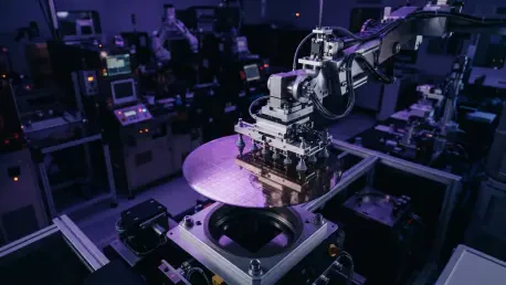
The technical boundary between “front-end” wafer fabrication and “back-end” assembly is rapidly disappearing, driven by the need for extreme precision in chip stacking. As advanced packaging moves toward wafer-level processes like 3D integration, it requires the same high-precision photolithography and cleanroom environments that were previously exclusive to silicon foundries. This has allowed major wafer fabs to capture a larger portion of the value chain by offering “all-in-one” manufacturing systems. By keeping the chip within a single ecosystem from the initial silicon print to the final 3D stack, foundries can reduce logistical complexity, minimize the risk of contamination during transport, and significantly improve overall yield. This integrated approach ensures that the most advanced AI chips are almost entirely finished before they ever leave the foundry’s control, fundamentally changing the role of traditional assembly and test providers in the high-end market.
In response to this encroachment, traditional assembly firms are moving “upstream” by mastering high-end packaging and micro-bump technologies that rival the precision of the foundries themselves. Rather than a total displacement of these firms, a new collaborative model is emerging where foundries and assembly specialists sign decade-long agreements to operate as a single, virtual production line. We see this in recent partnerships where wafer fabrication in one facility is seamlessly handed off to an adjacent advanced packaging plant owned by a separate firm. These facilities are often linked by shared software platforms and automated transport systems, effectively erasing the physical and operational gaps between the two companies. This level of integration allows for real-time feedback loops where data from the packaging process can be used to tune the wafer fabrication parameters, resulting in a continuous optimization of the manufacturing flow that was impossible under the old fragmented model.
Software-Driven Innovation and the Smart Foundry
Manufacturing in the AI era is no longer solely a matter of physics and chemistry; it is increasingly a software-defined process. Chip designers are now providing the “computational intelligence” required to optimize the actual execution of the foundry floor. For example, the astronomical amounts of data required for modern lithography masks are now processed using GPU-accelerated libraries that speed up calculations by as much as 50 times compared to traditional methods. This synergy means that the design company is no longer just a customer providing a blueprint; they are a technology partner providing the software tools that make the manufacturer more efficient. This marks a departure from the traditional client-vendor relationship, evolving into a shared research and development environment where software and hardware are co-optimized for maximum output. The foundry becomes a physical manifestation of the designer’s algorithmic efficiency, creating a tight feedback loop between code and silicon.
Beyond lithography, wafer fabs are now integrating advanced AI models for real-time visual inspection and process control on the factory floor. These models use massive datasets to predict potential defects before they occur, allowing for autonomous adjustments to the manufacturing equipment. This creates a technical synergy where the software tools provided by the designer directly enhance the yield and efficiency of the manufacturer. Digital twin technology has also become standard, allowing companies to simulate the entire manufacturing process in a virtual environment before a single wafer is processed. This capability is essential for the complex 3D architectures of 2026, where the margin for error is nearly zero. By integrating AI-driven inspection and simulation into the physical reality of silicon manufacturing, the industry has achieved a level of precision that was previously considered unreachable, demonstrating that the future of hardware is inextricably linked to the sophistication of the software that manages its creation.
Strategic Consensus: The Networked Integration Model
The transition toward a networked integration model reached a definitive state as the industry successfully abandoned the linear structures of the past. Companies that embraced deep capital integration and collaborative “co-opetition” found themselves at the center of the AI revolution, while those that clung to isolated operational silos struggled to maintain relevance. The shift established that having a superior design is secondary to having guaranteed, high-bandwidth access to the entire manufacturing stack. This period was marked by a strategic consensus that performance scaling now occurs at the system level through 3D integration rather than just through transistor shrinkage. The industry realized that the boundary between design and manufacturing had been permanently erased, replaced by a unified effort to push the limits of what silicon could achieve. This realization led to a new era of geographic realignment, where manufacturing clusters were built not just for cost efficiency, but for proximity to research hubs and regional supply security, funded by the very firms that designed the chips.
Moving forward, the industry must prioritize the standardization of interconnect protocols to ensure that this networked model remains sustainable and open to innovation. Stakeholders should focus on building resilient, multi-vendor ecosystems that allow for the seamless integration of logic, memory, and specialized accelerators from different sources. The actionable takeaway from this structural transformation is the necessity of long-term capital planning and the cultivation of deep technical partnerships that span the entire value chain. Organizations that treat their suppliers as strategic extensions of their own R&D departments will be best positioned to navigate the complexities of future computing nodes. As we look toward 2027 and beyond, the focus will likely shift to even more radical forms of integration, such as silicon photonics and heterogeneous chiplet architectures, which will require an even higher degree of collaboration. The era of the solitary semiconductor giant ended, replaced by a sophisticated web of global partnerships that collectively drive the advancement of artificial intelligence.