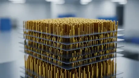

The persistent drive to shrink electronic components has finally encountered the unyielding boundaries of atomic physics, forcing engineers to reconsider the fundamental architecture of the modern microprocessor. For over half a century, the semiconductor industry successfully followed the trajectory of Moore’s Law by doubling transistor density through lithographic refinement, but this two-dimensional approach has reached a point of diminishing returns. As transistors approach the size of individual atoms, issues such as quantum tunneling and excessive heat leakage have turned traditional scaling into an uphill battle. The shift from a flat, expansive layout to a three-dimensional vertical structure represents a pivotal moment in engineering, akin to transforming a sprawling suburban landscape into a dense metropolis of high-rise skyscrapers. By stacking circuits vertically, researchers at the University of Illinois Grainger College of Engineering have unlocked a new dimension for growth, effectively bypassing the physical constraints that once threatened to halt the progress of global computing power.
The transition to vertical integration is not merely a matter of stacking existing chips but requires a complete rethink of how individual layers are fabricated and interconnected. In traditional planar designs, the speed of electricity is often hampered by the distance it must travel across a wide surface area. Vertical stacking minimizes these distances, allowing for faster communication and reduced power consumption. However, the complexity of building these “high-rise” chips has long been stymied by the extreme conditions required for silicon manufacturing. This breakthrough provides a sustainable path forward, ensuring that the next generation of processors can handle the massive data demands of the modern era without requiring a fundamental change in the materials that have powered the digital revolution for decades.
Overcoming the Heat Barrier in Semiconductor Manufacturing
Managing the Thermal Budget: Temperature Constraints in Stacking
The primary obstacle preventing the widespread adoption of vertical 3D integration has been the incompatible temperature requirements of different manufacturing stages, often referred to as the thermal budget. To create the high-quality single-crystalline silicon necessary for high-speed processing, fabrication facilities typically operate at temperatures exceeding 1,000 degrees Celsius. While the initial foundation of a chip can withstand such heat, adding a second or third layer of silicon using these methods would prove catastrophic for the circuitry below. The delicate copper or aluminum wiring that connects the transistors on the first layer would liquefy or warp long before the upper layers could be finalized, rendering the entire device useless. This has necessitated a strict thermal ceiling of approximately 400 degrees Celsius for any processing that occurs after the initial layer is established.
Staying below this 400-degree threshold is a non-negotiable requirement for protecting the integrity of the underlying metal interconnects. Engineers have spent years attempting to find a middle ground that allows for high-quality semiconductor growth without destroying the work already completed. The recent advancements from the Illinois research team demonstrate that it is possible to maintain the structural and electrical integrity of the base layer while successfully adding high-performance silicon on top. By developing a method that operates well within the safe thermal limits of existing metal wiring, they have removed the most significant technical barrier to monolithic 3D integration. This achievement ensures that the move to the third dimension does not come at the expense of the reliability and durability that consumers and industries expect from modern electronic components.
Reliability Standards: Selecting High-Performance Silicon Over Alternatives
In the quest to circumvent the thermal budget problem, many research teams previously experimented with alternative materials for the upper tiers of 3D chips, such as carbon nanotubes or various metal oxides. These materials were attractive because they could be deposited at much lower temperatures than traditional silicon, theoretically allowing for vertical stacking without damaging the foundation. However, these alternatives often introduced a new set of problems, including significantly lower electron mobility and inconsistent manufacturing yields. While they functioned in controlled laboratory settings, they lacked the raw performance and long-term reliability required for the high-stakes environments of data centers, autonomous vehicles, and advanced consumer electronics.
Relying on these exotic materials created a performance gap that made 3D integration less appealing for high-end applications where speed is paramount. The breakthrough at the University of Illinois shifts the focus back to single-crystalline silicon, which remains the gold standard for the semiconductor industry due to its predictable behavior and exceptional conductivity. By refining a technique to transfer high-quality silicon membranes onto an existing chip at low temperatures, the researchers have matched the performance of traditional 2D processors while gaining the density benefits of 3D architecture. This approach maintains a consistent material platform across all layers, simplifying the supply chain and ensuring that the final products meet the rigorous reliability standards established over the last few decades of semiconductor development.
Comparing Advanced Integration Techniques
Monolithic Construction: Improving Performance Over Wafer Bonding
Understanding the significance of this new approach requires a comparison with the current industry standard for 3D stacking, known as wafer bonding. In the wafer bonding process, two or more fully completed silicon wafers are manufactured separately and then aligned and fused together using sophisticated adhesives or direct bonding techniques. While this method is currently utilized in some memory and image sensor applications, it suffers from inherent precision issues. Even the most advanced equipment struggle to align these large wafers with perfect accuracy at the nanometer scale. This misalignment limits the number of vertical connections, known as Through-Silicon Vias, that can be made between the layers, effectively creating a data bottleneck that limits the overall speed of the chip.
Monolithic 3D integration, by contrast, builds each subsequent layer directly on top of the previous one in a sequential, bottom-up process. This eliminates the need for bonding two separate rigid surfaces and allows for the creation of vertical interconnects that are significantly smaller and more numerous. Because the layers are grown or transferred in place, the alignment is governed by lithographic precision rather than mechanical wafer handling. This results in a connection density that is 10 to 100 times higher than what is possible with wafer bonding. By removing the physical gap between layers and increasing the number of pathways for data to travel, monolithic designs offer a substantial improvement in bandwidth and a reduction in the power required to move information between logic and memory components.
Sequential Fabrication: Dense Connectivity and Vertical Precision
The sequential nature of monolithic fabrication allows for a level of design flexibility that was previously unthinkable in the semiconductor world. When building a chip layer by layer, engineers can place transistors and memory cells in a way that optimizes the thermal and electrical characteristics of the entire stack. This bottom-up construction means that the vertical wires connecting the tiers can be as small as the horizontal wires within a single layer. Such high-density connectivity is crucial for modern computing tasks that require the constant transfer of massive amounts of data, such as real-time video processing and complex simulations. The precision of this method ensures that signal latency is virtually eliminated, as the physical distance electrons must travel is reduced from millimeters to micrometers.
Moreover, the precision offered by sequential fabrication reduces the likelihood of manufacturing defects that often plague bonded wafers. In wafer bonding, a single misalignment can ruin two entire wafers, leading to significant waste and higher costs. Monolithic integration allows for more granular quality control throughout the build process, as each layer can be verified before the next is applied. This advancement not only improves the performance metrics of the chip but also enhances the economic viability of 3D manufacturing. By achieving such high levels of vertical precision, the industry can finally move away from the limitations of bonding and embrace a more integrated, efficient way of designing the hardware that underpins the digital economy.
The Technology Behind the Vertical Shift
Nanomembrane Innovation: The Transfer and Conformity Process
At the heart of this vertical breakthrough is the use of ultrathin silicon nanomembranes, which are engineered to be only 10 nanometers thick. These membranes are created on a separate donor wafer and then carefully “peeled” away using a specialized polymer stamp. The transfer process is conducted at room temperature, which completely avoids the high-heat requirements of traditional silicon growth. Because these membranes are so incredibly thin, they possess a unique flexibility that allows them to conform perfectly to the topography of the circuit layer below. This is a critical advantage, as traditional silicon wafers are rigid and brittle, making them prone to cracking or leaving air gaps when pressed against another surface that isn’t perfectly flat.
The rolling process used to apply these membranes ensures a uniform and defect-free interface between the layers. This technique effectively laminates the high-quality silicon onto the existing circuitry, creating a solid foundation for the next tier of transistors. The ability of the nanomembrane to adapt to the underlying structures ensures that there are no voids that could cause electrical failure or heat traps. This innovation transforms silicon from a rigid substrate into a versatile building material that can be layered repeatedly without compromising the integrity of the device. By mastering the physical properties of these membranes, the researchers have provided a practical solution for stacking high-performance materials in a way that was previously considered physically impossible.
Transistor Architecture: Solving Heat Issues with Junctionless Designs
Beyond the transfer of the silicon itself, the researchers had to reimagine the design of the transistors to accommodate the low-temperature environment. Standard transistor fabrication involves a process called “doping,” where impurities are injected into the silicon to change its electrical properties. This process usually requires an activation step involving temperatures near 1,000 degrees Celsius to ensure the impurities are properly integrated into the crystal lattice. To avoid this heat-intensive step, the team utilized “junctionless” transistors. In this configuration, the silicon membrane is pre-treated with the necessary impurities before it is transferred to the 3D stack. This allows the transistors to function efficiently without needing any high-temperature processing once they are in place on the chip.
The junctionless design is particularly well-suited for 3D integration because it simplifies the internal structure of the transistor. Instead of having distinct regions with different electrical charges, the entire channel of the transistor is uniformly doped. The flow of electricity is controlled by a metal gate that can “turn off” the entire channel through an electric field. This approach not only solves the thermal budget problem but also results in transistors that are highly efficient and less prone to the leakage currents that often affect traditional designs at very small scales. By combining nanomembrane transfer with junctionless architecture, the engineering team created a manufacturing workflow that is both physically viable and thermally safe, paving the way for more complex multi-layered processors.
Future Prospects and Industry Impact
Road to Commercialization: Industrial Scaling and Production Readiness
The successful demonstration of three-layered 3D structures with nearly 100% yield has caught the attention of the world’s leading semiconductor foundries. As the industry moves toward 2026 and beyond, the focus is shifting from laboratory experiments to large-scale production environments. Collaborative efforts with major players like Intel and TSMC are already underway to integrate these nanomembrane transfer techniques into existing fabrication lines. The goal is to move this technology from niche applications into high-volume manufacturing for consumer and enterprise hardware. Because the process uses industry-standard silicon and existing lithography tools, the barrier to adoption is significantly lower than it would be for entirely new material systems.
Scaling this technology involves refining the automated rolling and stamping processes to handle thousands of wafers per hour. Engineers are currently working on optimizing the speed of membrane transfer and ensuring that the electrical performance remains consistent across millions of individual chips. The potential for this technology to extend the life of Moore’s Law is immense, as it allows manufacturers to continue increasing transistor counts without needing to develop smaller and more expensive lithography machines. By building upward, the industry can maintain its historical pace of innovation while utilizing the infrastructure and expertise it has developed over the past several decades. This transition marks a sustainable evolution in hardware design that balances cutting-edge performance with manufacturing reality.
Artificial Intelligence: Breaking the Memory Wall with Vertical Stacking
One of the most profound impacts of monolithic 3D integration will be felt in the field of artificial intelligence, where the “memory wall” has long been a bottleneck for performance. In traditional 2D architectures, the physical distance between the processor and the memory chips causes significant delays in data retrieval, forcing the AI system to wait for information. By stacking memory layers directly on top of logic layers, 3D chips can drastically reduce this distance and increase the number of parallel connections between them. This vertical proximity allows for nearly instantaneous data access, which is essential for training large-scale language models and processing complex neural networks in real time.
The shift toward vertical stacking provided a necessary solution for the power-hungry demands of modern AI data centers. By reducing the energy required to move data across a chip, 3D integration makes high-performance computing more environmentally sustainable and cost-effective. The Illinois team demonstrated that their 3D transistors could match the speed of traditional high-temperature silicon, meaning there is no performance penalty for moving to a multi-tiered design. As this technology matured, it enabled a new class of “smart” devices that can perform advanced AI tasks locally, without needing to rely on distant cloud servers. This development represented a fundamental change in how computing power is distributed, ensuring that the next decade of digital growth is defined by efficiency, speed, and architectural innovation.