
The global semiconductor industry is currently navigating a critical transition period driven by an insatiable demand for processing power as society moves toward a future dominated by artificial intelligence, massive data centers, and sophisticated medical technologies. As the complexity of digital tasks increases, the need for smaller, faster, and more energy-efficient computer chips has never been more urgent for manufacturers striving to maintain technical superiority. Current extreme ultraviolet (EUV) lithography represents the absolute gold standard for etching these intricate circuits on silicon, yet the technology remains significantly hindered by staggering capital costs and mechanical complexities that limit its widespread accessibility. A new proposal from Professor Tsumoru Shintake at the Okinawa Institute of Science and Technology (OIST) aims to solve these issues by completely reimagining the optical path used in chip production. This research introduces a redesigned high numerical aperture (high-NA) system that promises to make manufacturing more precise while simultaneously lowering the barriers to entry for advanced high-performance computing.
The Mechanics of Modern Atomic Scale Lithography
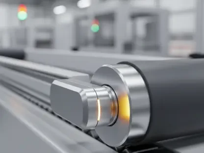
Extreme ultraviolet lithography utilizes light with a wavelength of only 13.5 nanometers, which is necessary because the features on modern silicon wafers are now measured at the atomic scale rather than the microscopic level. In a typical setup, light is guided through a series of specialized mirrors to a reflective photomask that contains the blueprint of the chip’s circuitry. When the light reflects off this mask, it carries the pattern through a projector that reduces the image size and focuses it onto the silicon wafer with extreme precision. This process requires a vacuum environment and incredibly expensive optics, as standard glass would absorb the light rather than refract or reflect it. The complexity of these machines makes them difficult to maintain and even harder to calibrate for mass production. Furthermore, the sheer size of the equipment requires massive facilities with specialized climate controls to prevent even the slightest deviation in the production cycle during operation.
Overcoming the Limitations of High Numerical Aperture
A primary metric for the effectiveness of these systems is the Numerical Aperture (NA), which describes the range of angles over which the system can accept or emit light to create fine patterns. While a higher NA allows for the resolution of significantly smaller features, it also introduces significant optical distortions known as mask 3D effects that plague modern chip production. These occur because light interacts with the three-dimensional structure of the mask at steeper angles, leading to blurring and shadowing that can compromise the performance of the finished hardware. Engineers have traditionally tried to compensate for these effects by adding more mirrors, but this only increases light loss and raises the energy requirements for the source. Each additional mirror surface absorbs about thirty percent of the light, meaning that complex systems require more powerful and expensive light sources to reach the wafer. This trade-off between resolution and efficiency has become a major roadblock for the industry.
A Radical Shift to In-Line Optical Alignment
To confront these physical limitations, Professor Shintake has proposed a radical departure from conventional zig-zag optical paths in favor of a much more efficient in-line configuration. In this model, the photomask, the projector mirrors, and the silicon wafer are all aligned along a single, straight optical axis to minimize light scattering and alignment errors. This simplified arrangement reduces the overall complexity of the machine and helps maintain the integrity of the light as it moves through the system, potentially solving many of the alignment issues found in current hardware. By removing the need for a complex series of angled reflections, the system can preserve more of the original light energy, which translates to faster processing times for each individual wafer. This shift represents a fundamental change in how lithography systems are built, moving away from the bulky designs of the past decade toward a more compact and manageable architecture that can revolutionize factory floor plans.
Eliminating Distortions Through Two-Stage Projection
The heart of this new architecture is a two-stage projection system that utilizes two sets of concave and convex mirror pairs to guide the light with unprecedented accuracy. By carefully calculating the reflections between these stages, the system can effectively cancel out the optical defects that typically occur at high resolutions and steep angles. This design ensures that the high numerical aperture is maintained for fine detail while simultaneously suppressing the distortive effects that have long plagued high-end semiconductor manufacturing processes. Because the light hits the mask at a near-perpendicular angle, the problematic shadowing effects are almost entirely eliminated without requiring the use of extremely high-power light sources. This optical trick allows for the creation of sharper images on the silicon, which results in fewer defective chips and a higher yield for manufacturers. The ability to maintain such high fidelity is essential for producing the dense transistor arrays used in next-generation hardware.
Disrupting the Economic Monopoly of Chip Production
One of the most compelling aspects of the OIST proposal is its potential to upend the economics of the semiconductor industry by drastically lowering the capital required for high-end fabrication. Currently, a single EUV lithography machine represents a massive capital investment for any company, often costing between $200 million and $300 million depending on the specific configuration. This high cost has created a significant bottleneck where only a handful of the world’s wealthiest companies can afford to produce the most advanced chips, effectively limiting competition and the pace of global innovation. For many medium-sized manufacturers, the transition to EUV has been financially impossible, forcing them to rely on older, less efficient technologies that cannot compete in the high-performance market. By introducing a design that simplifies the core mechanics of the machine, the industry could see a shift toward a more diverse ecosystem of chip producers and specialized startups.
Environmental and Efficiency Gains in Semiconductor Fab
Shintake’s design could potentially reduce equipment costs to approximately one-quarter of their current levels by simplifying the optical path and reducing the number of expensive mirrors. This reduction in complexity also means that maintenance costs would be significantly lower, as there are fewer specialized components that require frequent calibration or replacement. Furthermore, the chips produced by these systems are naturally more energy-efficient, helping to reduce the growing electricity demand and carbon footprint of global data centers. When the cost of manufacturing drops, the savings can be passed down to consumer electronics and specialized industrial equipment, making advanced technology more affordable for developing markets. The potential for a fourfold decrease in hardware costs would allow smaller players to enter the advanced chip market, fostering a more competitive environment. This competition is likely to drive even faster advancements in chip design as more engineers gain access to tools.
Material Science and the Precision Mirror Challenge
Despite the optimism surrounding these theoretical findings, the journey from a computational model to a functional factory floor is filled with engineering hurdles that must be overcome. The next phase involves building a physical prototype to prove the concept in a real-world environment, which requires manufacturing mirrors with near-perfect reflectivity and atomic-level smoothness. Achieving this level of precision is a monumental task that will require deep collaboration with materials scientists to ensure there are no defects on the mirror surfaces that could scatter the light. Even a single misplaced atom on the surface of a mirror can cause enough distortion to ruin a batch of wafers, making the fabrication of these optics one of the most difficult tasks in modern science. Researchers must also develop new coatings that can withstand the intense heat and radiation generated by the EUV light source over long periods without degrading, ensuring the longevity and commercial viability of the entire system.
Solving the Problems of Structural and Thermal Stability
Furthermore, the in-line design requires extreme structural stability to function correctly in a high-speed industrial setting where thousands of wafers are processed daily. Because the system handles such minute scales, even the slightest vibration from a nearby road or thermal expansion from the machine’s own heat could throw the mirrors out of alignment and ruin the silicon wafers. Therefore, the housing for the new projector must be as innovative as the optical path it contains, ensuring that the system remains perfectly calibrated during the high-speed manufacturing process. Engineers are looking into advanced active damping systems and specialized ceramic materials that do not expand or contract significantly with temperature changes. This level of environmental control adds another layer of complexity to the facility design, even if the machine itself is simpler. Ensuring that the entire assembly remains static at the nanometer level is a challenge that requires the integration of high-frequency sensors.
Strategic Implementation of Modular Production Standards
The conclusion of the research phase demonstrated that the theoretical limits of chip density could be pushed much further than previously thought by utilizing this streamlined optical approach. Stakeholders within the technology sector recognized the need for a paradigm shift in how lithography was funded and developed to avoid future supply chain bottlenecks. To move forward, industry leaders prioritized the development of open-source optical standards that used Shintake’s in-line configuration to foster a broader base of equipment suppliers. This strategy involved shifting investment from proprietary mirror designs toward shared material science research to solve the reflectivity challenges more quickly. Future considerations included the training of a new generation of lithography engineers who were proficient in managing these simplified yet highly precise systems. By focusing on modularity and accessibility, the industry successfully lowered the barrier to innovation for high-performance computing hardware.