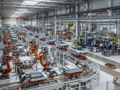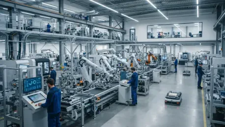

South Korean memory leaders are struggling to balance the modernization of Chinese operations with the strict export controls of the U.S. government. This delicate equilibrium is currently being tested as the global semiconductor landscape shifts under the weight of artificial intelligence and evolving national interests. By overhauling their massive fabrication facilities in mainland China, Samsung and SK Hynix are attempting to navigate a path that allows for technical progression without triggering regulatory backlash from Washington. The strategic pivot involves upgrading NAND flash memory production lines to exceed the 200-layer threshold, a move necessitated by the rapid rise of domestic competitors that have begun to dominate the local market. These industry giants are now forced to retool their existing infrastructure in Xian and Dalian, transforming older manufacturing lines into high-performance hubs capable of satisfying the immense storage demands of the modern era.
Market Shift: The Rise of Yangtze Memory Technologies
The shift in market dynamics within mainland China has reached a critical tipping point that neither Samsung nor SK Hynix can afford to ignore. For the first time in the history of the memory industry, a domestic Chinese firm, Yangtze Memory Technologies Co. (YMTC), has successfully overtaken its South Korean rivals in their own backyard. During the second quarter of 2026, YMTC captured a staggering 38.5% of the regional NAND flash market, a significant leap from the 28% share it held just one year prior. This surge has come at a direct and painful cost to the established leaders; Samsung’s market share dipped from 36% to roughly 33.5%, while SK Hynix witnessed a decline from 20% to 17%. The rapid ascent of YMTC is not merely a statistical anomaly but a reflection of a maturing domestic ecosystem that is increasingly capable of meeting high-performance storage needs. To reclaim their standing, these firms must modernize their local operations or risk being permanently sidelined in a vital region.
AI Revolution: The Economic Necessity of High-Density Storage
The push for higher layer counts in memory architecture is no longer just a matter of technological prestige; it is a fundamental requirement for economic survival in the burgeoning era of artificial intelligence. As global data centers and premium mobile devices demand ever-greater density and speed, the reliance on legacy production cycles has become a liability for firms operating in China. High-capacity solid-state drives are the backbone of AI-driven infrastructures, and without the ability to produce advanced memory with high layer counts, Samsung and SK Hynix would find themselves locked out of the most lucrative contracts. By pushing their Chinese plants toward the 286-layer mark, these companies aim to provide the hardware performance necessary to compete with YMTC’s homegrown innovations, such as their successful 232-layer designs. This technological arms race highlights the necessity of maintaining a competitive edge in fabrication efficiency to ensure the firms remain the primary suppliers for the next generation of data.
Project Monami: Retrofitting Samsung’s Xian Production Lines
Samsung’s primary counteroffensive in this shifting landscape is concentrated at its massive production complex in Xian, which serves as a cornerstone of its global operations by accounting for approximately 40% of its total NAND flash output. Under the internal banner of “Project Monami,” the company is systematically transitioning its existing lines from 192-layer chips to the cutting-edge 286-layer V9 architecture. A central tenet of this strategy is the focus on retrofitting existing equipment and infrastructure rather than pursuing greenfield expansions that would involve building entirely new facilities. By upgrading current tools and optimizing established production lines, Samsung is attempting to stay within the narrow confines of current international export regulations while still achieving a significant boost in technological capability. The roadmap for this transition is ambitious, with the Xian plant slated to process 40,000 wafers per month by the close of 2027 to meet the global demand for high-end AI hardware.
The Dalian Transition: Modernizing SK Hynix’s Manufacturing Hub
Parallel to the efforts in Xian, SK Hynix is undertaking an equally significant overhaul of its facility in Dalian, a site that has become central to the company’s long-term strategy following its acquisition from Intel. This facility, operating under the Solidigm brand, currently produces 192-layer chips but is in the process of transitioning to 240 layers or higher. The importance of the Dalian site cannot be overstated, as it serves as the sole manufacturing hub for Solidigm and plays a pivotal role in the subsidiary’s plans for a public offering in the United States. SK Hynix is pursuing a dual-track strategy by seeking authorization to conduct research and development for architectures exceeding 300 layers while simultaneously maintaining its existing Chinese footprint. This approach is intended to create a robust technical foundation that can eventually be transitioned to manufacturing operations on American soil, balancing immediate production with future growth prospects in Western markets.
Geopolitical Compliance: Navigating United States Export Controls
The success of these technical upgrades is inextricably linked to the evolving trade policies and export controls managed by the United States Commerce Department’s Bureau of Industry and Security. Since the implementation of strict regulations on advanced semiconductor equipment, such as specialized etching tools, foreign firms have had to operate under renewable licenses. The regulatory environment has grown increasingly complex, with authorities signaling a reluctance to authorize capacity expansions for foreign-owned plants located within China. Consequently, Samsung and SK Hynix have shifted their focus toward technical upgrades of existing capacity, which allows them to improve chip density without violating the ban on new projects. This regulatory pressure inadvertently created a window of opportunity for YMTC, which has successfully scaled high-layer designs and is already yielding small batches of 294-layer memory, forcing the South Korean leaders to move with even greater urgency in their domestic retrofitting.
Strategic Conclusion: Balancing Global Innovation and Security
To protect their valuable intellectual property, both Samsung and SK Hynix established a clear technological hierarchy that distinguished their overseas operations from their domestic headquarters. While the plants in China were modernized to the 240-286 layer range to remain commercially viable for AI data center contracts, the truly bleeding-edge innovations remained strictly within South Korean borders. At home, Samsung demonstrated prototypes featuring more than 400 layers, and SK Hynix marketed finished memory products that reached the 321-layer threshold. This tiered approach ensured that the most advanced technologies remained anchored in their home country, providing a strategic buffer against potential technology transfer. Moving forward, the successful deployment of these 200-layer-plus architectures ensured that the South Korean firms remained indispensable in the global supply chain while strictly adhering to international trade regulations and maintaining their competitive edge over local rivals.