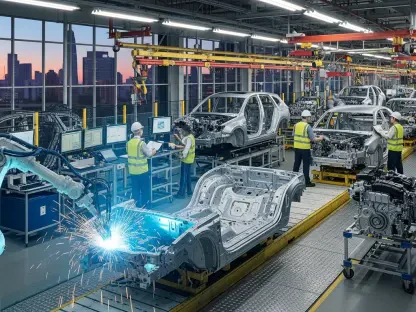

While the pristine cleanroom captures the public eye, the chaotic symphony of machinery humming beneath the floorboards dictates the true success of modern microchip production. This hidden layer, known as the subfab, is undergoing a radical transformation as the industry moves toward 2nm processes and beyond. Modern fabrication requires more than just lithography; it demands an intricate web of support systems that manage extreme pressures and hazardous byproducts.
The Engine Room: Defining the Subfab Infrastructure
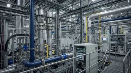
The semiconductor subfab is the critical infrastructure layer located directly beneath the cleanroom floor, housing the auxiliary systems required to maintain high-volume manufacturing. This technology encompasses a complex network of vacuum pumps, gas abatement systems, and chemical management units that ensure the process tools above function correctly. As chip architectures shrink and complexity increases, the subfab has evolved from a simple utility space into a sophisticated environment where the most energy-intensive and chemically hazardous stages of production are managed.
Core Components: Operational Frameworks and Specialized Support
Technical Systems: Vacuum, Abatement, and Chemical Delivery
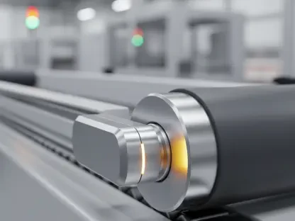
At the heart of subfab infrastructure are the systems that manage the extreme environments required for wafer processing. Vacuum pumping systems are essential for creating the low-pressure conditions necessary for deposition and etching, while advanced gas abatement systems neutralize toxic and greenhouse gas byproducts before they are released. These components must operate with high reliability to prevent downtime in the cleanroom, making their performance metrics vital to the overall throughput of the facility.
Service Models: The Infrastructure-as-a-Service Model in Subfab Research
A significant technical shift is the emergence of the Infrastructure-as-a-Service model, where third-party providers design, build, and own the physical subfab infrastructure. This approach allows semiconductor manufacturers and equipment suppliers to access high-volume manufacturing conditions without the massive capital expenditure required for proprietary pilot lines. By providing a neutral, shared environment, this model facilitated the generation of compliance-ready data and the validation of new equipment under real-world operating parameters.
Pre-Competitive Collaboration: Emerging Shifts in Research
The most notable shift in the subfab landscape is the movement toward pre-competitive collaboration to address sustainability and workforce development. Historically, subfab operations were siloed and proprietary, but the increasing cost of environmental compliance and technical complexity has driven industry leaders to share research resources. New initiatives focused on green subfab technologies, such as plasma-based abatement and water recycling systems, which are developed through partnerships between research labs, infrastructure owners, and global foundries.
Modern Deployment: Real-World Applications in Chip Manufacturing
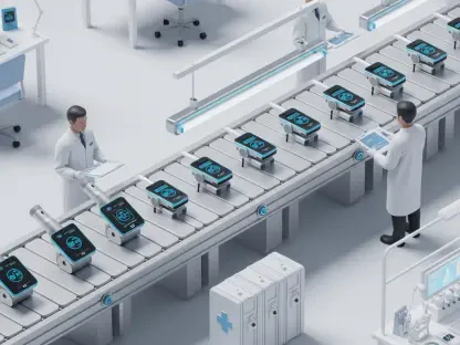
The deployment of advanced subfab infrastructure is most evident in the latest 3nm and 2nm logic and memory fabs. These facilities use the subfab as a testing ground for materials reclaim processes, where precious or hazardous chemicals are captured and reused to lower costs and reduce environmental impact. Additionally, original equipment manufacturers use these specialized facilities to validate the performance of next-generation process tools before they are integrated into commercial production lines, ensuring that new technologies meet stringent uptime and safety standards.
Overcoming Obstacles: Technical Hurdles and Market Pressures
Despite its importance, the subfab faces significant challenges regarding the industry’s massive carbon footprint and the high cost of upgrading legacy facilities. Integrating modern abatement and energy-efficient pumping systems into existing subfabs requires complex retrofitting and significant downtime. Furthermore, managing intellectual property within shared environments remains a concern for competing manufacturers. Ongoing efforts to mitigate these issues included the use of government incentives, such as the U.S. CHIPS Act and EU Horizon programs, which provided the funding necessary to modernize the back-end of manufacturing.
Future Outlook: The Subfab as a Center for Innovation
The trajectory of subfab technology points toward an era of total automation and environmental stewardship. Future developments are expected to include AI-driven predictive maintenance for vacuum and abatement systems, further reducing energy consumption and unexpected failures. As the industry moves toward net-zero goals, the subfab will transition from a hidden utility layer into a center for technological innovation, where the circular economy of semiconductor manufacturing is realized through advanced chemical and energy recovery systems.
Strategic Verdict: Summarizing the Value of Subfab Infrastructure
This review demonstrated that the subfab was no longer a secondary consideration but a primary driver of fab sustainability. The transition to shared research facilities provided a clear path for smaller players to innovate without the burden of massive overhead. Stakeholders focused on developing modular abatement units that allowed for rapid scaling as production demands shifted. Ultimately, the industry moved toward a decentralized model that prioritized environmental metrics alongside wafer throughput, ensuring that the next generation of chips did not come at an unsustainable ecological price.