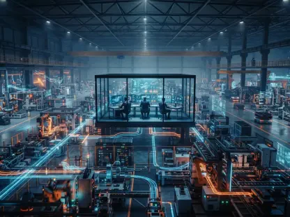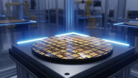

The global semiconductor landscape has shifted dramatically as Semiconductor Manufacturing International Corporation successfully demonstrates that extreme ultraviolet lithography is not the only path toward achieving high transistor density in modern silicon fabrication. While industry leaders previously deemed EUV essential for scaling below the seven-nanometer threshold, recent advancements in N+3 technology have challenged this paradigm by pushing deep ultraviolet systems to their absolute physical limits. This development signals a significant pivot for the industry, as it proves that sophisticated architectural optimizations and refined multi-patterning techniques can compensate for the lack of shorter-wavelength light sources. By utilizing these methods, engineers have managed to shrink feature sizes to a level once thought impossible without the billion-dollar machinery controlled by a handful of nations. The resulting chips exhibit transistor density that competes directly with 5nm and early 3nm class nodes produced by competitors using more advanced equipment. This achievement highlights a resilient engineering approach that prioritizes process ingenuity over hardware acquisition.
Technical Foundations: Precision Engineering for DUV
The transition to the N+3 process relies heavily on the mastery of self-aligned quadruple patterning, a technique that allows for the creation of features far smaller than the wavelength of the immersion DUV light itself. By meticulously depositing and etching multiple spacer layers around a single patterned mandrel, the foundry can effectively double or quadruple the resolution of the original lithographic pass. This iterative process requires an extraordinary degree of control over etch selectivity and material deposition uniformity to prevent the accumulation of overlay errors that typically plague complex multi-patterning schemes. Furthermore, the integration of advanced deposition tools and high-precision metrology has allowed for the correction of minor deviations in real-time during the fabrication cycle. These refinements have yielded a logic density that rivals EUV-based nodes, providing a viable alternative for high-performance computing and mobile applications. The success of this approach is rooted in a deep understanding of thin-film chemistry and mechanical engineering, rather than just optical scaling.
In addition to patterning innovations, the N+3 node incorporates significant improvements in FinFET transistor architecture and interconnect scaling to maximize performance within the density constraints. Designers have focused on reducing the contact resistance and improving the gate-all-around-like characteristics even within a standard FinFET framework to ensure that the power-performance-area metrics remain competitive. By optimizing the middle-of-line layers and utilizing cobalt or ruthenium for critical interconnects, the process mitigates the traditional RC delay issues associated with shrinking metal pitches. This holistic view of the manufacturing process ensures that the increased density does not lead to excessive heat or power leakage, which are common hurdles when pushing DUV to its limits. The capability to manufacture such dense arrays without EUV also provides a unique cost-benefit profile, as the older DUV machines are more widely available and have more mature maintenance ecosystems. Consequently, this allows for a more flexible production schedule and a reduction in the capital expenditure per wafer once the yields are fully stabilized across high-volume production runs.
Market Dynamics: Global Resiliency and Scaling
The emergence of N+3 as a viable contender in the advanced logic space has forced a reevaluation of global export controls and the effectiveness of technology bottlenecks intended to stall domestic chip development. With the ability to produce high-density semiconductors domestically, the reliance on external foundries for critical infrastructure components has begun to diminish, creating a more self-reliant technological ecosystem. This shift is particularly evident in the telecommunications and artificial intelligence sectors, where the demand for dense logic continues to outpace the availability of leading-edge capacity. As these domestic nodes mature from 2026 to 2028, the secondary market for older DUV equipment is likely to see increased demand as other manufacturers attempt to replicate these complex multi-patterning successes. This creates a diversified supply chain where the absolute cutting edge is no longer the only viable path for high-end electronic design. The strategic resiliency gained from this process cannot be overstated, as it ensures a steady supply of advanced silicon regardless of the geopolitical tensions surrounding the supply of EUV lithography systems.
As the industry looked beyond the immediate hurdles of 2026, the focus shifted to refining the yield management systems for these hyper-complex multi-patterning environments. Foundries invested heavily in AI-driven defect inspection and predictive maintenance to ensure that the increased number of process steps did not lead to unsustainable waste. This commitment to operational excellence allowed manufacturers to maintain competitive pricing even as the number of exposures per wafer increased. The broader adoption of these techniques proved that the path to advanced computing was more varied than previously theorized. Stakeholders across the supply chain coordinated to ensure that the design rules for N+3 were accessible to a wider array of global partners, promoting a standard that balanced density with manufacturability. This collaborative effort effectively bridged the gap between legacy DUV capabilities and the high-performance requirements of modern technology. Ultimately, the industry learned that while hardware remained a critical component, the true driver of advancement was the creative application of existing tools to solve seemingly insurmountable physical challenges through meticulous engineering and strategic planning.