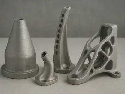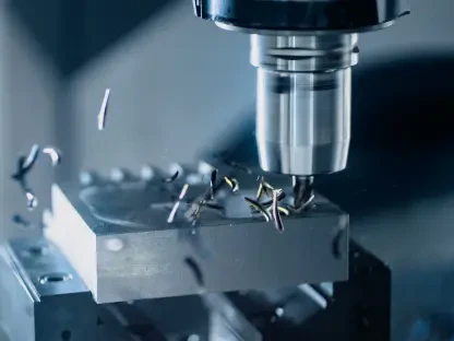

The long lead times associated with custom micro-injection molding are being reduced from months to days through the adoption of rapid micro-additive prototyping. This shift comes at a critical juncture for the semiconductor and micro-electronics industries, where the relentless drive toward miniaturization has collided with the physical realities of legacy fabrication. For decades, engineers relied on Computer Numerical Control (CNC) machining and micro-injection molding to produce the housings, connectors, and structural elements of electronic devices. However, these subtractive and formative processes are inherently limited by the geometry of cutting tools and the requirements of mold extraction. As components shrink into the sub-millimeter range, the mechanical stresses of traditional manufacturing often cause delicate parts to warp or fail during production. This silicon ceiling has forced designers to compromise on performance for the sake of manufacturability, a trade-off that is increasingly unacceptable in a market demanding more power in smaller footprints. By adopting micro-precision additive manufacturing, the industry is moving toward a period where the design is dictated by the intended function of the device rather than the limitations of the factory floor, essentially rewriting the rules of what can be physically built.
Overcoming Traditional Geometric Constraints
Precision Engineering: The Mechanics of PµSL
Projection Micro Stereolithography, or PµSL, serves as the technological backbone of this manufacturing revolution by operating on a scale that standard additive manufacturing cannot reach. While industrial-grade systems typically struggle with resolutions below fifty microns, PµSL achieves precision at the single-digit micron level, enabling the production of parts with features smaller than a human hair. This method involves the use of a digital light processing engine to project an entire layer of a part onto a vat of photosensitive resin, polymerizing the liquid into a solid voxel by voxel. Because the process is additive, it does not suffer from the line of sight restrictions that plague CNC machining. Designers can create intricate internal geometries, such as hollow channels or complex lattice structures, that provide incredible strength-to-weight ratios without the need for secondary support structures that would be impossible to remove from a micro-scale part. This level of dimensional control allows for the production of sharp corners, smooth vertical walls, and ultra-thin membranes that were previously inaccessible through traditional molding.
By controlling the polymerization process at such a granular level, engineers can ensure that every microscopic feature is exactly where it needs to be, reducing the variance that often leads to electrical interference or mechanical instability in high-performance electronics. The voxel-based construction method allows for a degree of complexity that was once considered a liability in the manufacturing world. In the past, every additional hole, groove, or internal cavity added cost and time to the production cycle, but with PµSL, complexity is essentially free. This allows for the iterative testing of radical designs that would have been cost-prohibitive just a few years ago. Engineers are now utilizing these capabilities to prototype micro-mechanical sensors and high-density connectors with internal geometries that optimize signal flow and mechanical interlocking. The precision afforded by this technology ensures that the transition from a digital model to a physical component is nearly perfect, which is a prerequisite for the high-frequency and high-speed applications that dominate the current technological landscape.
Vertical Innovation: Breaking the Planar Prison
A fundamental limitation of traditional electronic design is its reliance on two-dimensional layouts, often referred to by industry experts as the planar prison. For years, the architecture of printed circuit boards and their associated components has been dictated by flat layers and linear interconnects. PµSL technology shatters this paradigm by allowing for the three-dimensional routing of both signals and fluids within a single component. In this environment, an electrical path or a microfluidic channel is no longer restricted to a single plane or a simple vertical via; it can wind, spiral, and branch through the X, Y, and Z axes simultaneously. This flexibility is transformative for the development of high-density interconnects, where the ability to route around obstacles or through the center of a structural element can significantly reduce the overall footprint of a device. The ability to use the full three-dimensional volume of a component for functional routing allows designers to bypass the congestion often found in modern mobile devices and wearable sensors.
Furthermore, this three-dimensional routing capability facilitates the creation of complex fluidic systems for lab-on-a-chip applications, where multiple chemical reactions or sensing operations must occur in a highly compact space. By utilizing the vertical dimension as effectively as the horizontal, designers can pack more functionality into a given volume, leading to a new generation of medical implants that are smaller and more capable than anything produced using legacy planar techniques. This architectural shift also impacts signal integrity, as 3D routing can be used to maintain precise distances between sensitive traces, reducing cross-talk and electromagnetic interference. The departure from flat-layer thinking allows for the design of integrated systems where the structural housing itself acts as a conduit for data and power. As electronic devices continue to shrink toward invisible form factors, the ability to utilize internal 3D space becomes the primary differentiator between successful innovation and a failed design that cannot be manufactured.
Enhancing Performance: The Power of Part Consolidation
Holistic Development: Shifting from Assembly to Integration
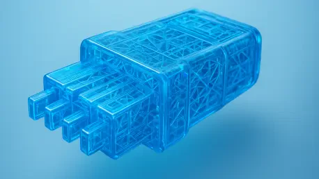
The transition from assembly-based design to integrated, performance-based design marks one of the most significant shifts in the history of electronic manufacturing. In a traditional workflow, a complex device is the sum of dozens or hundreds of discrete parts, each manufactured separately and then painstakingly assembled by hand or robotic systems. This process is not only expensive and time-consuming but also introduces the risk of tolerance stack-up, where the tiny margins of error in each individual part accumulate until the final product fails to meet its operational specifications. Micro-3D printing solves this by enabling part consolidation, the practice of printing multiple functional elements as a single, monolithic structure. When a connector, a housing, and a cooling channel are printed as one piece, the points of failure associated with joints, seals, and adhesive layers are virtually eliminated. This approach ensures that every feature remains perfectly aligned throughout its lifecycle, which is vital for micro-electronics where a deviation of even ten microns can lead to failure.
By moving away from the assembly-centric models of the past, manufacturers are finding that they can produce more reliable and durable products while simultaneously cutting the costs associated with supply chain management and labor-intensive production lines. This consolidation also allows for the creation of geometries that would be impossible to join through welding or fastening. For instance, internal baffles and supports can be grown within a part as it is being printed, providing structural integrity that is superior to a bolted or glued assembly. This structural homogeneity is particularly useful in environments subject to vibration or thermal expansion, as there are no disparate materials or mechanical interfaces to stress or separate over time. The economic benefits are equally compelling, as reducing the number of parts leads to simplified inventory management and a lower bill of materials. As companies seek to optimize their manufacturing footprints, the ability to print a fully integrated, multi-functional component in a single step provides a clear path toward leaner and more efficient production cycles.
Technical Application: Advancing High-Frequency and Thermal Systems
High-frequency applications, specifically those found in 5G and emerging 6G infrastructure, present a unique set of challenges that micro-precision 3D printing is uniquely equipped to handle. As the frequency of a signal increases, the physical size of the components required to manage that signal must decrease, and the precision of their internal surfaces becomes paramount. In radiofrequency engineering, the smoothness and geometry of internal wave-guiding structures directly influence the efficiency of signal transmission; even minor surface roughness or misalignment can cause significant loss. PµSL allows for the creation of internal corrugations and complex antenna geometries that are impossible to machine in a single piece. These monolithic antennas provide a cleaner signal path by eliminating the seams found in traditional multi-part assemblies. The precision of micro-additive manufacturing ensures that these intricate internal structures meet the strict tolerances required for millimeter-wave communication, where accuracy is measured in microns.
Simultaneously, the thermal demands of these high-performance systems are escalating as devices consume more power in smaller spaces. Modern micro-additive techniques allow for the embedding of 3D microfluidic cooling channels directly into the walls of a device or adjacent to the most heat-intensive components. This ensures that heat is dissipated at the source through liquid or air cooling, preventing the thermal throttling that often limits the performance of modern electronics. The ability to integrate these high-performance thermal features into a single, compact part provides a competitive edge in an industry where speed and efficiency are the primary markers of success. Beyond thermal management, this technology is also being used to create specialized electromagnetic interference shielding that is integrated directly into the component’s geometry. By combining high-frequency signal management with advanced cooling and shielding in one printed part, engineers can achieve a level of system optimization that was previously hindered by the limitations of traditional, separate-part manufacturing methods.
Practical Validation: Real-World Impacts and Future Structures
Practical Evidence: Validating Technology through Case Studies
The real-world efficacy of micro-precision printing is best illustrated by recent successes in the production of millimeter-wave antennas and high-precision fiber optics. In one notable application, manufacturers collaborated to produce corrugated horn antennas that are essential for high-bandwidth data transmission in satellite and telecommunications systems. Historically, these antennas were manufactured by machining multiple sections and then brazing or bolting them together, a process that frequently introduced internal gaps and alignment errors. By utilizing PµSL technology, the entire antenna was printed as a single unit with a highly complex internal structure that maintains strict dimensional tolerances throughout its length. After the printing process, the part was subjected to a specialized conformal metallization, which deposited a thin, highly conductive layer over the plastic substrate. This resulted in an end-use component that was not only lighter and more cost-effective than its metal counterpart but also demonstrated superior signal performance.
These case studies have shifted the industry’s perception of 3D printing from a tool reserved for making visual prototypes to a legitimate manufacturing method for mission-critical components. The ability to move from a digital design to a fully functional, metallized micro-part in a matter of days has fundamentally changed the risk assessment for many engineering firms, encouraging more radical innovation. In the field of photonics, the technology has been used to create fiber array guides that require sub-micron precision to ensure light is coupled efficiently between fibers. These parts are now being produced with internal geometries that allow for tighter packing and better signal integrity than traditional micro-machined parts. The success of these applications proves that micro-additive manufacturing can handle the rigors of end-use environments, providing a scalable solution for the most demanding technical challenges. As more firms adopt these workflows, the empirical data gathered from these real-world implementations will continue to drive the optimization of materials and printing parameters.
Strategic Evolution: Redefining the Future of Electronic Layouts
As micro-precision 3D printing becomes more integrated into the standard engineering toolkit, it is prompting a total redesign of electronic architecture that mimics the complexity of biological systems. Rather than viewing a device as a box filled with flat boards and wires, engineers are beginning to design 3D electronics where the internal structure functions like the vasculature of a living organism. In this model, electrical pathways, thermal vents, and structural supports are interwoven in a way that maximizes every cubic millimeter of space. This architectural freedom enables the creation of custom parts per design, allowing engineers to move away from the limitations of off-the-shelf connectors that often force awkward layouts or increased device volume. Because micro-3D printing removes the high upfront costs and ten-week lead times associated with custom micro-injection molds, it is now economically viable to create a bespoke connector or housing for every specific application.
This capability is particularly disruptive for the development of medical diagnostics and wearable sensors, where the shape of the device must conform to the human body or specific anatomical features. By treating the entire volume of a device as usable space for electronic and mechanical routing, the industry is moving toward a state where the distinction between a device’s packaging and its circuitry is increasingly blurred, leading to unprecedented levels of integration and performance. This evolution also supports the growing trend of decentralized manufacturing, where custom parts can be printed on-site or in smaller, localized facilities, reducing the reliance on massive, centralized production hubs. The ability to produce high-performance, custom-fit components on demand will likely change the competitive dynamics of the consumer electronics market, favoring companies that can iterate quickly and tailor their products to niche consumer needs. This strategic evolution is not just about making parts smaller; it is about rethinking the fundamental relationship between a device’s form and its functional requirements.
The adoption of micro-precision 3D printing represented a pivotal moment when the electronics industry finally moved beyond the constraints of traditional manufacturing. The analysis demonstrated that by embracing additive techniques like PµSL, engineering teams successfully reduced their development cycles from months to a few days, facilitating more frequent iteration and faster time-to-market. The transition to performance-based design allowed for the consolidation of complex assemblies into monolithic parts, which improved mechanical reliability and drastically reduced signal loss in high-frequency applications. Organizations that integrated these methods into their workflows found that they were no longer bound by the rigid rules of mold-pull or tool reach, enabling the creation of compact, high-density devices that were previously impossible to build. For engineers looking to maintain a competitive advantage, the path forward involves a fundamental shift in how internal structures are conceived, prioritizing the three-dimensional routing of signals and integrated thermal management from the earliest stages of the design process. The successful implementation of these technologies in end-use components proved that micro-additive manufacturing is the necessary foundation for the current era of miniaturization. By focusing on the functional requirements rather than the limitations of the fabrication process, the industry established a new standard for precision, efficiency, and design freedom in the modern electronic landscape. Moving forward, the integration of conductive materials directly into the printing process will likely eliminate the need for secondary metallization, further streamlining the path from digital concept to finished product.