
Tesla’s Optimus humanoid robot and Cybercab fleet require specialized processors that prioritize energy efficiency and low-latency data processing over standard commercial chip features. This specialized demand has driven the establishment of Terafab, a centralized semiconductor manufacturing ecosystem in Grimes County, Texas, intended to achieve total vertical integration for some of the world’s most ambitious technology projects. Rather than relying on generic, off-the-shelf silicon that often carries unnecessary overhead, the new facility allows for the creation of bespoke chips tailored specifically for neural network training and real-time inference. This initiative signals a departure from the traditional fabless model, where companies design chips but outsource the actual manufacturing to distant foundries. By controlling every stage from the initial architectural layout to the final packaging, the project aims to eliminate the delays and supply chain vulnerabilities that have historically hindered high-volume production of advanced robotics and electric vehicles. The scale of the investment, which surpassed $16 billion in its initial phase, reflects a strategic commitment to technological sovereignty in an era where the control of high-end processing power is synonymous with economic and industrial leadership. Consequently, Terafab serves as both a production hub and a research laboratory, pushing the boundaries of what is possible in automated manufacturing and silicon density.
The Economic Ambition: Rivaling National GDPs
The projected economic footprint of the Terafab facility is so vast that its internal output is expected to rival the Gross Domestic Product of a top-20 global economy. While comparing a single corporate project to the entire industrial production of a mid-sized nation sounds like hyperbole, it reflects the unprecedented concentration of value in the high-end semiconductor market. As silicon becomes the foundational resource for every sector from transportation to telecommunications, a facility capable of producing over a terawatt of AI computing capacity annually effectively becomes a central engine for global growth. This concentration of manufacturing power in Texas positions the region as a primary node in the digital infrastructure of the late 2020s. By capturing the entire value chain of semiconductor production, the initiative ensures that the economic benefits—from high-paying engineering roles to the secondary service industries that support a massive industrial site—remain localized within the American industrial landscape, creating a self-sustaining cycle of wealth and innovation that few other private ventures have ever attempted.
Beyond the direct financial metrics, the global scale of this project influences how international markets value artificial intelligence and autonomous systems. When a single facility can dictate the supply of the world’s most advanced AI processors, it gains the power to influence industry standards and pricing models across the globe. This level of dominance suggests a future where technological leaders are measured not just by their software or consumer products, but by their raw manufacturing capacity. Terafab’s goal is to transition from being a consumer of technology to a primary provider of the underlying infrastructure that makes modern life possible. This shift effectively places the facility at the heart of a new industrial revolution, where data processing power is treated with the same strategic importance as energy production or steel manufacturing. The ripple effects of this ambition are already being felt in global stock markets, as investors recalibrate their expectations for the automotive and aerospace industries based on which companies can guarantee their own access to the silicon chips required to function in an increasingly automated world.
Strategic Synergy: Powering the Earth and the Stars
The collaboration between Tesla and SpaceX within the Terafab framework is a logical progression of a management philosophy centered on shared resources and cross-disciplinary innovation. Both companies face a common challenge: the need for high-density, energy-efficient computing that can survive and perform in environments where traditional hardware often fails. While Tesla focuses on the terrestrial challenges of autonomous driving and humanoid labor, SpaceX looks toward the vacuum of space and the complex requirements of orbital communications. By merging these requirements into a single fabrication site, both organizations can leverage shared research into advanced materials and transistor architectures. This synergy allows for the development of “dual-use” silicon that is as rugged as it is powerful, ensuring that the same underlying technology that drives a car through a busy intersection can also manage the telemetry of a spacecraft during a Mars landing. This unified approach to hardware development significantly reduces the research and development costs that would be incurred if each company pursued its own independent silicon strategy.
For Tesla, the primary focus remains the scaling of the Optimus robot and the expansion of the Cybercab network, both of which rely on continuous real-time data processing. The chips produced at Terafab act as the central nervous system for these machines, enabling them to interpret visual data and navigate complex environments with human-like precision. Simultaneously, approximately 75% of the facility’s eventual output is slated for SpaceX missions, specifically the Starlink satellite constellation and the infrastructure required for deep-space exploration. These orbital processors must be radiation-hardened and capable of dissipating heat in the absence of an atmosphere, a technical requirement that is often overlooked by commercial chipmakers. By internalizing the production of these specialized components, SpaceX ensures that its mission timelines are never held hostage by the production schedules of external vendors. This strategic alignment turns Terafab into a versatile powerhouse capable of supporting the most demanding applications on the planet and beyond, creating a closed-loop system of innovation that accelerates the pace of development for both companies.
Infrastructure: Building the Texas Technology Hub
Selecting Grimes County, Texas, as the location for Terafab was a deliberate move to capitalize on the state’s rapid transformation into a global center for heavy industry and advanced technology. The region offers a unique combination of a business-friendly regulatory environment, a robust energy grid, and a growing pool of technical talent migrating from traditional tech hubs. The project is bolstered by a $30 million grant from the Texas Enterprise Fund, signaling a strong public-private partnership aimed at securing the future of American manufacturing. This local support is critical, as a facility of this magnitude requires more than just capital; it needs a supportive local infrastructure capable of providing the massive amounts of stable electricity and ultra-pure water essential for semiconductor fabrication. The development of Terafab is expected to catalyze a broader industrial expansion in the area, drawing in suppliers and specialized service providers who want to be in close proximity to the world’s most advanced silicon foundry. This geographic concentration of expertise creates a “gravity well” for innovation, further solidifying the region’s status as the new frontier of the technology sector.
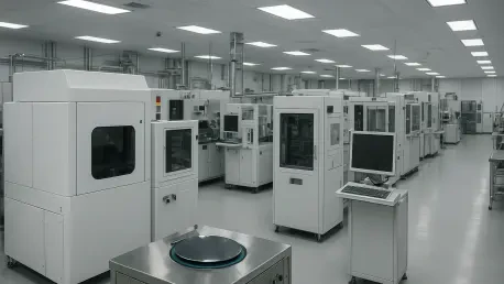
Constructing a semiconductor fabrication plant is widely regarded as one of the most complex engineering feats a company can undertake. These facilities require “clean rooms” with air filtration systems thousands of times more effective than those found in modern hospitals, as even a microscopic speck of dust can ruin an entire wafer of processors. Furthermore, the sensitivity of the lithography equipment requires foundations that are completely isolated from external vibrations, ensuring that the precision of the manufacturing process remains undisturbed. The $16.8 billion allocated for the first phase of Terafab covers the massive logistical challenge of installing these systems and building the specialized power substations required to keep the plant running 24/7. As the facility scales, the regional infrastructure in Texas will undergo a parallel evolution, with new transportation links and residential developments emerging to support the thousands of engineers and technicians who will call this hub home. This transformation of the rural landscape into a high-tech heartland demonstrates the sheer power of industrial vision when backed by significant capital and local political will.
Industry Partnerships: Collaboration Amidst Independence
Despite the overarching goal of technological independence, the Terafab initiative recognizes that the semiconductor industry is far too complex for any single entity to master without specialized partners. The involvement of Intel, which joined the project in early 2026, has been instrumental in bridging the gap between visionary design and practical, high-volume manufacturing. Intel’s “Foundry” model provides the technical expertise and established “recipes” for silicon fabrication that take years, if not decades, to develop from scratch. This collaboration allows Tesla and SpaceX to focus on the architecture of their proprietary chips while leveraging Intel’s sophisticated packaging technologies and manufacturing workflows. This hybrid approach—designing in-house but manufacturing with the help of established titans—accelerates the timeline for getting functional chips into the field. It represents a pragmatic acknowledgment that even the most innovative companies benefit from the deep institutional knowledge held by veterans of the silicon industry, ensuring that Terafab hits its production targets without falling victim to the common pitfalls of new fabrication ventures.
Beyond the domestic partnership with Intel, there is significant potential for deeper cooperation with the Taiwan Semiconductor Manufacturing Company, the global leader in advanced node fabrication. Discussions regarding a “co-location” model, where TSMC could lease space or manage specific production lines within the Terafab complex, suggest a new way of thinking about international technical cooperation. Such an arrangement would provide Tesla and SpaceX with immediate access to the latest transistor technologies, such as two-nanometer and sub-nanometer processes, which are essential for staying at the cutting edge of AI performance. This strategy allows the Texas facility to operate at the frontier of semiconductor physics while maintaining the security and logistical benefits of a domestic site. By integrating these global leaders into the Terafab ecosystem, the initiative ensures that it remains competitive with the best foundries in Asia and Europe. This network of partnerships creates a robust foundation for the project, combining Musk’s disruptive drive with the proven reliability of the world’s most experienced chipmakers, ultimately resulting in a manufacturing capability that is both innovative and exceptionally stable.
Technological Frontiers: Intelligence at the Edge and in Orbit
At its core, the Terafab project is a factory for intelligence, producing the hardware that will define the capabilities of artificial intelligence for years to come. The emphasis on high-density AI processing signals a future where computing power is no longer a scarce resource but a fundamental utility available for a wide range of applications. For the Tesla Optimus robot, this means having a local “brain” capable of processing complex visual and tactile data without needing to constantly check in with a central server. This “edge computing” capability is essential for safety and efficiency, allowing robots to make split-second decisions in dynamic environments like factory floors or private homes. The custom silicon produced at Terafab is specifically optimized for these neural network tasks, offering a level of performance-per-watt that general-purpose processors cannot match. This advantage is what will ultimately make humanoid robotics a viable and cost-effective solution for labor shortages, as the machines become smarter and more energy-efficient with each new generation of chips produced in the Texas foundry.
The ambitions of the project extend far above the Earth’s surface, as the facility prepares to supply the processors required for the next generation of orbital data centers. By moving data processing into space, SpaceX aims to revolutionize global internet services, providing high-speed, low-latency connectivity to every corner of the planet. However, operating hardware in the vacuum of space presents unique challenges, including extreme temperature fluctuations and constant exposure to cosmic radiation. Terafab’s role is to produce the ultra-reliable, radiation-hardened components that can operate for years without the possibility of manual repair or maintenance. These orbital nodes will act as a decentralized cloud network, providing secure data storage and processing power that is physically removed from terrestrial threats. The successful deployment of these systems depends entirely on the ability to manufacture specialized hardware that can withstand the rigors of the space environment while maintaining high levels of performance. In this way, Terafab is not just supporting existing industries; it is creating the technological foundation for an entirely new off-planet economy that could redefine our relationship with data and connectivity.
Overcoming Technical and Economic Hurdles
The transition from a blueprint to a fully operational semiconductor fab is fraught with technical risks that can derail even the most well-funded projects. In the world of high-end fabrication, the “yield”—the percentage of working chips on each silicon wafer—is the ultimate metric of success. A minor fluctuation in power, a microscopic leak in a chemical delivery system, or a slight error in the lithography process can lead to massive financial losses and production delays. Maintaining high yields requires a level of operational discipline and precision that is difficult to sustain over long periods, especially when pushing the boundaries of miniaturization. Furthermore, the capital intensity of the semiconductor industry means that Terafab must engage in a cycle of continuous reinvestment. To stay relevant, foundries must upgrade their multi-billion-dollar equipment every few years as new manufacturing nodes become standard. This creates a perpetual financial burden that requires a steady and massive stream of revenue to justify, making the long-term success of the facility dependent on the continued growth of the AI and robotics sectors.
Beyond the internal manufacturing challenges, the facility remains deeply embedded in a complex global supply chain for raw materials and specialized equipment. While the goal is vertical integration, Terafab still relies on external suppliers for high-purity silicon, rare earth minerals, and the sophisticated photolithography machines produced by companies like ASML. Any disruption in these specialized supply lines could halt production regardless of how well the facility itself is managed. Additionally, the project faces a significant challenge in talent acquisition, as there is currently a global shortage of semiconductor engineers with the expertise required to run a leading-edge foundry. To succeed, Terafab must compete with established giants like Nvidia, AMD, and Samsung to attract the world’s brightest minds. This “war for talent” is being fought not just with salaries, but with the promise of working on the most exciting and impactful projects in the world. The ability to recruit and retain this highly specialized workforce will be the ultimate factor in whether Terafab becomes a global leader or remains a bold but unrealized ambition within the larger Musk corporate empire.
Strategic Implications: A Blueprint for Technical Sovereignty
The Terafab initiative established a precedent for how private enterprises might navigate the increasingly fragmented landscape of global trade and industrial production. By internalizing the means of production for the most critical component of the modern era, these companies moved beyond the traditional limitations of vendor-managed hardware. Observers noted that the long-term viability of this model depended heavily on the sustained growth of the robotics sector and the successful deployment of large-scale orbital arrays. Stakeholders within the technology industry recognized that the next logical step involved the creation of decentralized, cross-industry standards that would allow smaller firms to tap into the specialized fabrication capabilities developed at the Texas site. Furthermore, the initiative demonstrated that the traditional separation between automotive, aerospace, and computing companies had effectively dissolved into a single, unified field of high-performance engineering. This convergence suggested that future market leaders would be those who could manage the entire stack of technology, from the raw silicon to the final autonomous behavior of a machine.
The successful launch of the Texas facility provided a clear roadmap for other nations and corporations looking to secure their own technological futures. It showed that while the barriers to entry in the semiconductor industry were incredibly high, they were not insurmountable for those with a long-term vision and significant capital. Policy experts pointed out that the public-private partnership model used in Texas could be replicated in other regions to bolster national security and economic resilience. As the project moved into its steady-state production phase, the focus shifted toward optimizing the recycling of silicon and reducing the environmental impact of large-scale fabrication. This commitment to sustainability, combined with the drive for technological dominance, ensured that the facility remained at the center of the global conversation regarding the ethics and mechanics of progress. Ultimately, the Terafab initiative proved that the path to the future was paved with silicon, and those who controlled the foundry controlled the direction of human innovation for the next several decades.