
The global semiconductor landscape is witnessing a seismic transformation as the pursuit of sub-2nm process nodes pushes the physical limits of traditional silicon fabrication beyond what conventional methods can sustain. As manufacturing reaches these microscopic thresholds, the margin for error effectively vanishes, necessitating a move toward intelligence-driven production environments. The strategic collaboration between NVIDIA and TSMC serves as the primary catalyst for this shift, merging accelerated computing with advanced lithography to redefine the modern foundry. By embedding artificial intelligence into every layer of the manufacturing stack, these industry leaders are transitioning from static hardware-centric models to dynamic, software-defined ecosystems. This evolution allows for the processing of astronomical datasets in real-time, ensuring that the next generation of high-performance chips can be produced with the precision and speed required to meet the escalating demands of the global AI economy through 2027 and beyond.
The Evolution: Computational Lithography and Mask Design
Computational lithography has historically been the most computationally intensive phase of chip design, often requiring massive server farms running for weeks to calculate a single mask pattern. The integration of the NVIDIA cuLitho library into TSMC’s workflow has fundamentally altered this timeline by offloading these massive mathematical workloads to specialized GPU architectures. This shift allows for a performance increase of up to 40 times compared to traditional CPU-based processing, enabling the creation of intricate curvilinear masks that were previously deemed impossible to manufacture. By significantly reducing the cycle time for mask production, the partnership ensures that the design-to-production pipeline remains agile even as circuit patterns become increasingly complex. Consequently, this acceleration reduces the overall carbon footprint of the fabrication process by minimizing the power consumption typically associated with months of continuous CPU-based computation, setting a new benchmark for sustainable high-tech manufacturing.
Molecular Innovation: Accelerated Material Science and Chemistry
Beyond the immediate challenges of lithography, identifying the physical properties of new chemical compounds for transistor gate materials represents a critical bottleneck for future node development. Utilizing the NVIDIA cuEST library, TSMC engineers are now able to simulate electronic structures and molecular interactions with a level of granularity that was once theoretically possible but practically unreachable. These simulations operate up to 50 times faster than conventional methods, allowing researchers to sift through thousands of potential material candidates to find those with the best thermal conductivity and energy efficiency. This rapid iteration is essential for developing the 2nm and 1.4nm nodes, where the choice of dielectric materials directly impacts the performance of the entire semiconductor industry. The ability to predict how materials behave at an atomic level before physical testing begins saves millions in research costs and prevents the delays that often plague the introduction of new manufacturing standards into the global market.
Yield Optimization: Real-Time Machine Learning and Telemetry
Maintaining high yields in a modern semiconductor facility requires the constant monitoring of hundreds of thousands of sensors that generate a continuous stream of telemetry data. TSMC has implemented CUDA Machine Learning, commonly known as cuML, to process these data flows instantaneously, allowing for the detection of subtle anomalies that might indicate a drift in calibration. Instead of waiting for a batch to fail inspection, the system can provide predictive insights that allow engineers to adjust machine parameters on the fly, thereby preserving the integrity of expensive silicon wafers. This level of granular oversight is particularly important as chips become more dense, where even a slight variation in chemical deposition or temperature can ruin an entire production run. By leveraging accelerated machine learning, the foundry can maintain a steady output of high-quality components, ensuring that the supply chains for everything from data center accelerators to consumer electronics remain stable and predictable during periods of high demand.
Automated Inspection: Vision Artificial Intelligence and Quality
Visual inspection remains a cornerstone of quality assurance, but the scale of modern chips requires an automated approach that exceeds human capability. The deployment of the NVIDIA Metropolis platform and the TAO Toolkit has enabled TSMC to build highly specialized vision AI models that perform defect inspection at a nanometer scale. These models are trained to recognize even the smallest microscopic fractures or impurities that could lead to circuit failure after the chip is packaged. A key advantage of this system is its inherent flexibility; as production processes change or new designs are introduced, the AI can be retrained quickly using synthetic data to adapt to new visual patterns. This ensures that the inspection process does not become a bottleneck in the high-speed production line. By automating these once-manual tasks, the partnership has achieved a level of precision that guarantees nearly perfect uniformity across millions of units, which is a prerequisite for the reliable deployment of AI hardware in mission-critical infrastructure.
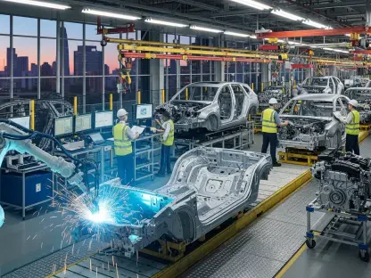
Operational Excellence: Digital Twins and Logistics Optimization
The transition to virtual-first manufacturing was solidified by the adoption of NVIDIA Omniverse, which allowed TSMC to create comprehensive digital twins of their fabrication facilities. These FabTwins provided a simulated environment where engineers optimized robotic movements and wafer logistics using ##00 GPUs to solve complex spatial puzzles. This implementation resulted in significantly reduced bottlenecks and higher tool utilization rates across the production floor. Moving forward, the industry adopted more rigorous standards for real-time data interoperability to ensure these AI-driven systems remained scalable as demand increased. Organizations seeking to emulate this success prioritized the modernization of their data infrastructure and the training of personnel in GPU-accelerated simulation tools. By focusing on software-defined operational efficiency rather than just physical capacity, manufacturers ensured that their facilities remained resilient against supply chain fluctuations. This paradigm shift proved that the future of semiconductor production relied as much on algorithmic sophistication as it did on physical engineering.