
The continent’s semiconductor landscape is transforming as designers and manufacturers replace fragmented production silos with a cohesive digital thread that spans the entire chip lifecycle. This fundamental shift reflects a growing realization that localized manufacturing capacity alone cannot guarantee technological independence in a volatile global economy. Instead, European leaders are prioritizing an integrated continuum where data flows seamlessly from early-stage design centers to the final delivery of silicon to end-users. By connecting these once-isolated phases, the region aims to build an industrial infrastructure that is both resilient to external shocks and capable of rapid innovation. This evolution represents more than a technical upgrade; it is a strategic repositioning of Europe as a global leader in high-end semiconductor production. As the industry moves away from transactional relationships toward deep-rooted collaborative networks, the emphasis is now on creating a self-sustaining ecosystem that supports every aspect of advanced electronics.
Strategic Foundation: The European Chips Act and Economic Realignment
The European Chips Act has emerged as the primary catalyst for this massive regional transformation, channeling over forty-three billion euros into projects intended to double the region’s share of the global market. While the financial commitment is substantial, the true value of this initiative lies in its role as a strategic blueprint for cross-border alignment and industrial self-sufficiency. By coordinating investments across various member states, the policy prevents the duplication of efforts and ensures that every part of the semiconductor value chain receives the necessary support to thrive. This coordinated approach is essential for competing with established manufacturing hubs in North America and East Asia, where government support has historically been more centralized. The focus is not just on building new factories, but on creating an environment where domestic startups and established giants can collaborate on cutting-edge research and development to push the boundaries of physics.
European enterprises are moving aggressively to mitigate the risks associated with an over-reliance on foreign manufacturing centers by developing their own integrated toolchains and internal supply routes. This transition is driven by the need for operational efficiency and the desire to protect intellectual property within a secure and regulated regional framework. In the current geopolitical climate, the ability to maintain a steady flow of high-end silicon is seen as a prerequisite for national and economic security. Therefore, the shift toward a sovereign ecosystem is not merely a matter of economic preference but a strategic necessity for maintaining the region’s industrial relevance. By establishing a robust internal network, European manufacturers can offer greater reliability to their customers in the automotive, industrial, and telecommunications sectors. This stability is becoming a key differentiator for the “Made in Europe” brand, attracting global companies that seek to diversify their supply chains away from high-risk regions.
Operational Evolution: Implementing Smart Factories and Digital Twins
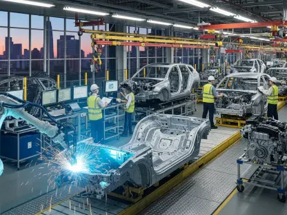
The transition from policy goals to physical reality is increasingly evident in the high-profile semiconductor projects currently operational across Germany, France, and Austria. These facilities are designed as data-driven nerve centers that utilize advanced artificial intelligence and high-level automation to monitor every aspect of the production process in real-time. By deploying sensors throughout the cleanroom, manufacturers can analyze production yields with unprecedented precision and perform predictive maintenance before equipment failures occur. This level of oversight allows firms to detect minute anomalies that would have previously gone unnoticed, thereby preventing expensive downtime and significantly reducing energy consumption. These “smart factories” represent the gold standard for modern electronics production, combining high-speed output with the flexibility needed to handle complex, low-volume orders. This technological leap ensures that European fabs remain competitive despite higher labor costs compared to other regions.
Beyond the physical automation of the factory floor, the industry is seeing a widespread adoption of virtual optimization techniques through the use of sophisticated digital twins. These virtual replicas of both the product and the manufacturing process allow companies like NXP to test and refine designs in a simulated environment before committing any resources to physical production. This approach dramatically reduces the likelihood of errors and optimizes resource use by identifying potential bottlenecks in the fabrication process before the first wafer is even processed. By leveraging these simulations, European chipmakers can accelerate the time-to-market for advanced silicon products, giving them a critical edge in sectors where innovation cycles are measured in months rather than years. The integration of digital twins into the development cycle also facilitates better collaboration between design teams and manufacturing engineers, ensuring that new chips are optimized for manufacturability from the very beginning.
Regulatory Landscape: Navigating Ethics and Environmental Standards
European semiconductor firms face the unique challenge of balancing rapid technological development with the world’s most stringent regulatory and environmental frameworks. As these companies integrate AI into their workflows for complex tasks like yield optimization and circuit layout, they must ensure their systems remain explainable and auditable. This requirement for human oversight and transparency is a cornerstone of the regional approach to technology, distinguishing European innovation from more opaque models found elsewhere. Maintaining high ethical standards is not seen as a hindrance but as a way to build long-term trust with global partners and consumers. By prioritizing governance alongside technical performance, the region is establishing a sustainable model for the deployment of artificial intelligence in heavy industry. This focus on “trustworthy AI” ensures that the automation of the semiconductor sector does not come at the expense of safety, security, or the loss of critical human expertise in the process.
Environmental sustainability has become a non-negotiable component of the European chip strategy, placing intense pressure on manufacturers to scale up while reducing their carbon footprints. This creates a “dual challenge” where companies must innovate at a blistering pace to stay ahead of global competitors while simultaneously leading the way in resource efficiency and waste reduction. Firms are investing heavily in water recycling technologies and renewable energy sources to power their energy-intensive fabrication processes. Successfully navigating these requirements is essential for maintaining the reputation of the European industrial base as a leader in responsible manufacturing. By demonstrating that high-tech production can coexist with aggressive climate goals, the region is setting a new global benchmark for the semiconductor industry. This commitment to green manufacturing also aligns with the broader goals of the European Green Deal, ensuring that the transition to a digital economy does not undermine the continent’s environmental objectives.
Future Pathways: Establishing Resilient Industrial Standards
The most significant obstacle to achieving full semiconductor sovereignty was the widening talent gap that threatened to slow the ambitious timelines set by regional policymakers. This transition to highly automated, AI-driven ecosystems required a workforce that possessed a rare blend of skills spanning traditional hardware engineering, data science, and software development. There was a voracious demand for professionals who could navigate these overlapping disciplines to manage the complex digital infrastructure that now defined modern fabrication plants. Universities and industry leaders responded by creating specialized training programs and apprenticeships designed to cultivate the next generation of semiconductor experts. Addressing this human capital shortage was just as important as securing financial investment, as the success of the ecosystem ultimately depended on people. Strategic partnerships became the new standard for industry success as specialized service providers provided the digital scaffolding necessary to bridge the gap between hardware and software.
To maintain this hard-won sovereignty, the regional industry focused on diversifying its talent pipelines and deepening its commitment to circular economy principles within the fab. Leaders moved beyond simple manufacturing by investing in domestic chemical and substrate production, ensuring that the entire bill of materials remained within a secure sphere of influence. Future efforts were directed toward the expansion of this integrated model into emerging fields like quantum computing and power electronics for electric vehicles. By continuously refining the digital thread that connected design to distribution, the continent stayed ahead of global shifts in demand and technology. The focus remained on fostering a culture of open innovation where small and medium-sized enterprises could contribute to the larger ecosystem without being sidelined by larger conglomerates. These steps ensured that the European semiconductor industry was not just a collection of factories, but a living network capable of adapting to any disruption.