
The migration of cryogenic characterization to the fab floor signals a new era of disciplined, data-driven manufacturing for extreme-environment electronics. For decades, the pursuit of quantum supremacy and superconducting logic was confined to the whisper-quiet halls of university physics departments, where liquid helium dewars and hand-wired dilution refrigerators were the tools of the trade. In those early days, success was defined by the singular “hero” device—a lone qubit or Josephson junction that exhibited perfect coherence or switching speeds despite a sea of surrounding failures. However, as the industry enters 2026, the stakes have evolved from basic scientific discovery to the brutal requirements of commercial scalability. The semiconductor landscape is now witnessing a fundamental transformation in how extreme-cold electronics are validated. Transitioning from small-scale academic setups to the robust infrastructure of the modern fabrication facility allows companies to treat quantum chips not as fragile laboratory specimens, but as mass-produced industrial components.
Industrializing Wafer-Level Characterization: From One to Millions
The industrialization of cryogenic testing focuses on the manufacturability of quantum components rather than just their basic operation. By utilizing automated wafer-level characterization, manufacturers can gather massive datasets that reveal how semiconductor process variations impact performance at extreme temperatures. These variations are often invisible at room temperature but become critical performance bottlenecks when a device is cooled to its operational state of 4 Kelvin. Moving to wafer-scale testing allows developers to identify systematic trends across a production run, such as performance gradients between the center and the edge of a wafer. In a research setting, a few successful devices might be enough for a paper, but in a fab, the entire wafer must meet strict standards. Automated probing ensures that these outliers are identified early, allowing for the establishment of manufacturing controls that guarantee repeatability across thousands of devices during the current production cycles.
Transitioning to full-wafer analysis represents a departure from the qualitative assessments of the past toward a more quantitative, statistical framework. When engineers probe hundreds of structures across 200 mm silicon-on-insulator or gallium arsenide wafers, they uncover the subtle nuances of lithographic drift and etching non-uniformity. These factors, while manageable in traditional CMOS production, have outsized effects on the delicate phase transitions and superconducting thresholds required for quantum logic. By capturing thousands of data points per wafer, the industry can finally establish “golden” performance metrics that define what a healthy device looks like before it is ever packaged. This rigorous approach effectively weeds out defective chips early in the cycle, preventing the massive waste associated with packaging and cooling devices that were doomed from the start. This level of scrutiny is essential for any facility aiming to achieve the yields necessary for the next generation of high-speed computing.
Hardware Innovations: Bridging the Cryogenic Gap
The shift toward the fab environment is largely facilitated by advanced hardware platforms designed to bridge the gap between experimental research and high-volume manufacturing. Tools such as modern automated cryogenic probe stations, including systems like the IQ3000, now enable Process Control Monitoring and the validation of Process Design Kits at cryogenic scales. These platforms allow for “Yield Learning,” a sophisticated feedback loop where testing data is used to fine-tune the etching, deposition, and lithography stages of the fabrication process in real-time. By providing a stable environment for 150 mm and 200 mm wafers, these machines permit the measurement of thousands of devices in a single cooling cycle. This capability is fundamentally different from the laborious process of mounting individual chips on sub-mounts, which characterized the previous era of development. Today, the focus is on providing high-speed electrical connectivity that can withstand the thermal contraction of components.
Establishing a reliable Process Design Kit at cryogenic temperatures is perhaps the most significant milestone for fab-based testing. Designers require accurate models of how transistors, resistors, and capacitors behave at 4 Kelvin to create complex circuits that function correctly on the first pass. Without the high-throughput data provided by modern fab-level testing stations, these models would remain based on theoretical extrapolations rather than empirical reality. Hardware innovations now allow for the characterization of noise figures, gain, and power consumption at extreme temperatures with the same level of precision expected in traditional electronics. This data enables the creation of design rules that account for the unique physics of super-cooled matter, such as increased carrier mobility or altered thermal conductivity. As these hardware platforms become more integrated into the fabrication line, they serve as the ultimate gatekeepers for manufacturing readiness, ensuring that every design is backed by physical measurements.
The Automation Revolution: Enabling High-Throughput Cycles
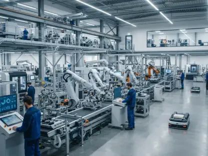
Automation is the defining feature of the move from lab to fab, as manual thermal cycling and probe alignment are far too slow for industrial needs. Automated systems eliminate human error and ensure that measurements are consistent and repeatable across different wafers and production lots. This high-throughput approach shifts the focus from flexible experimentation to the generation of a robust statistical distribution of device performance. In a manual lab setting, the simple act of aligning a probe tip to a ten-micron pad at 4 Kelvin could take an hour of careful adjustment due to thermal drift. In a modern automated system, machine vision and precision actuators handle these tasks in seconds, maintaining alignment even as the temperature fluctuates. This speed is what makes it possible to characterize an entire 200 mm wafer in hours rather than weeks, providing the rapid feedback that process engineers need to optimize their tools and maintain high levels of throughput.
As a technology nears the production phase, understanding the unique “signature” of a specific fabrication line becomes vital for long-term success. High-volume data management allows manufacturers to predict yields with high accuracy and identify the specific characteristics of their processes that may lead to failure. This disciplined approach ensures that the transition to commercial manufacturing is backed by a data-driven understanding of how the hardware behaves under extreme stress. By analyzing the performance distribution across hundreds of wafers, engineers can distinguish between random noise and systematic errors. For example, if a specific deposition chamber consistently produces higher-performing junctions, automation allows this trend to be spotted and replicated across the entire facility. This level of insight was impossible in the era of manual testing, where the sample size was too small to draw meaningful conclusions about the stability of the fabrication equipment or the consistency of the chemical precursors.
Temperature Correlation: The Path to Streamlined Yields
A significant frontier in this field is the effort to correlate room-temperature data with cryogenic performance to streamline the development cycle. If a reliable relationship can be established between a device’s behavior at 300 Kelvin and 4 Kelvin, room-temperature testing can serve as a fast and cost-effective screening tool. Building the massive datasets required to uncover these hidden correlations is only possible through the high-volume testing now occurring in fab environments. While some parameters, such as gate leakage or interconnect resistance, may change predictably, others involve complex quantum effects that only emerge at low temperatures. By performing side-by-side comparisons of wafer maps at both temperature extremes, researchers are developing machine learning models that can predict cryogenic success based on ambient-temperature electrical signatures. This predictive capability could eventually reduce the need for cryogenic testing by up to eighty percent, drastically lowering the cost of production.
The economic model of cryogenic testing is also changing, with “Test-as-a-Service” options becoming more prevalent to lower the barrier to entry for smaller developers. Since building a world-class cryogenic facility requires immense capital investment and a team of specialized technicians, many companies are leveraging external specialized labs for production-level testing. This ecosystem allows startups to focus on qubit design and software while utilizing the industrial-grade infrastructure necessary to prove their hardware is ready for the market. These external services provide access to the latest automated probe stations and data analysis suites, allowing smaller players to compete with established giants. Furthermore, this centralized testing approach helps standardize measurement protocols across the industry, ensuring that a qualified wafer from one foundry meets the same rigorous standards as one from another. This democratization of high-end testing is accelerating the pace of innovation, as it allows for faster iteration cycles.
Scaling the Future: Actionable Steps for Industry Integration
The successful integration of cryogenic testing into the fab floor established a new benchmark for manufacturing readiness within the quantum sector. By moving away from the isolated validation of individual devices, the industry adopted a holistic view of the semiconductor supply chain that prioritized reliability and scale. The transition was marked by significant investments in automated infrastructure, which allowed for the first time a true statistical understanding of superconducting device physics across entire 200 mm wafers. These efforts resulted in the creation of comprehensive design libraries that paved the way for more complex architectures and higher-density qubit arrays. The data collected during these initial phases provided the empirical evidence needed to convince investors and stakeholders that quantum hardware was ready for the rigors of a commercial environment, moving beyond the theoretical promises that had previously defined the field during its early development.
Moving forward, the industry prioritized the standardization of cryogenic interfaces to ensure interoperability between different cooling systems and silicon foundries. The next actionable steps involved the deployment of standardized Process Control Monitoring structures that could be used across multiple fabrication sites to verify tool health at 4 Kelvin. As technology progressed from 2026 to 2028, the establishment of industry-wide benchmarks was finalized to transform quantum computing into a reliable, mass-market utility. This required a shift toward collaborative data-sharing models where foundries and designers worked together to refine the cryogenic Process Design Kits. By treating the cryogenic environment as a standard manufacturing variable rather than an experimental obstacle, the semiconductor industry successfully bridge the gap between scientific theory and industrial reality. These systemic changes ensured that the next generation of high-performance computing was built on a foundation of repeatable, high-yield manufacturing processes.